
EECE 290 Exam 1 with Solution, Spring 2011
American University of Beirut · Analog Signal Processing · 7 pages · with solution

More EECE 290 files
- Exam 1 Clean Copy · Spring 2019ExamView
- Exam 2 Clean Copy · Spring 2019ExamView
- Exam 1 with Solutions · Spring 2019Exam · with solutionView
- Exam 2 with Solutions · Spring 2018Exam · with solutionView
- Exam 1 with Solutions · Spring 2018Exam · with solutionView
- Exam 1 Quiz 1 2016 · Spring 2017ExamView
- Exam 2 Quiz 2 2016 · Spring 2017ExamView
- Exam 1 · Spring 2017ExamView
Show the text of this exam
p1/7
EECE 290 Analog Signal Processing – Quiz 1
March 12, 2011
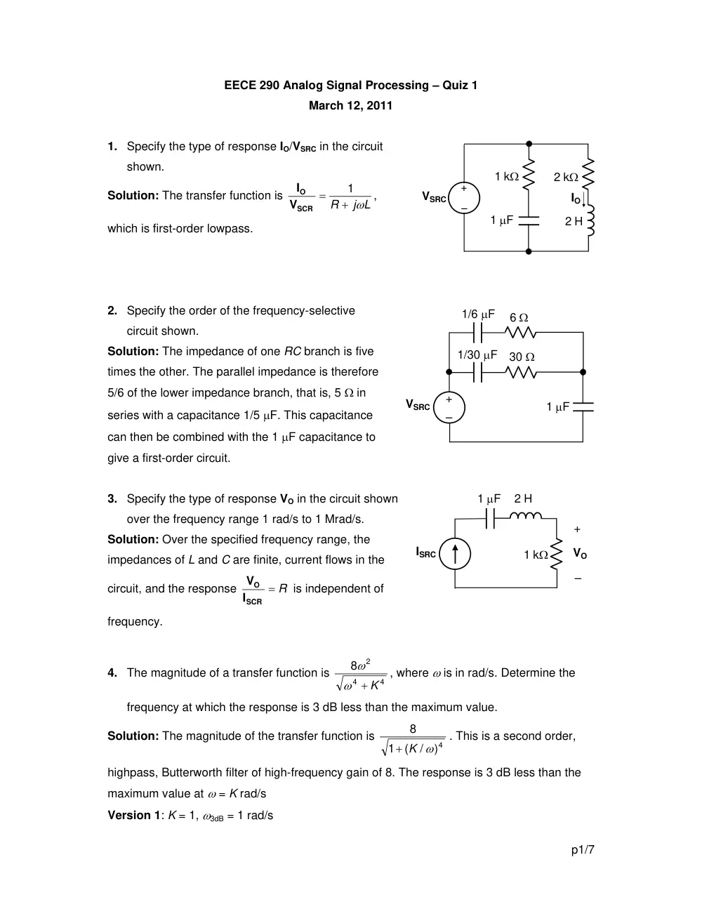
1. Specify the type of response IO/VSRC in the circuit
shown.
Solution: The transfer function is
j L
R
+ ω
=
1
SCR
O
V
I
,
which is first-order lowpass.
2. Specify the order of the frequency-selective
circuit shown.
Solution: The impedance of one RC branch is five
times the other. The parallel impedance is therefore
5/6 of the lower impedance branch, that is, 5 Ω in
series with a capacitance 1/5 μF. This capacitance
can then be combined with the 1 μF capacitance to
give a first-order circuit.
3. Specify the type of response VO in the circuit shown
over the frequency range 1 rad/s to 1 Mrad/s.
Solution: Over the specified frequency range, the
impedances of L and C are finite, current flows in the
circuit, and the response
R
=
SCR
O
I
V
is independent of
frequency.
4. The magnitude of a transfer function is
4
4
2
8
+ K
ω
ω
, where ω is in rad/s. Determine the
frequency at which the response is 3 dB less than the maximum value.
Solution: The magnitude of the transfer function is
4)
/
(
1
8
+ K ω
. This is a second order,
highpass, Butterworth filter of high-frequency gain of 8. The response is 3 dB less than the
maximum value at ω = K rad/s
Version 1: K = 1, ω3dB = 1 rad/s
–
+
VSRC
6 Ω
1/6 μF
30 Ω
1/30 μF
1 μF
–
+
VSRC
1 μF
1 kΩ
IO
2 kΩ
2 H
`
ISRC
1 μF
1 kΩ
–
+
VO
2 H
p2/7
Version 2: K = 2, ω3dB = 2 rad/s
Version 3: K = 3, ω3dB = 3 rad/s
Version 4: K = 4, ω3dB = 4 rad/s
Version 5: K = 5, ω3dB = 5 rad/s
5. Determine the slope of the low-frequency asymptote of the transfer function of the
preceding problem.
Solution: At low frequencies, the magnitude of the transfer function is
2
2
8 ω
K
. The slope is
+40 dB/decade.
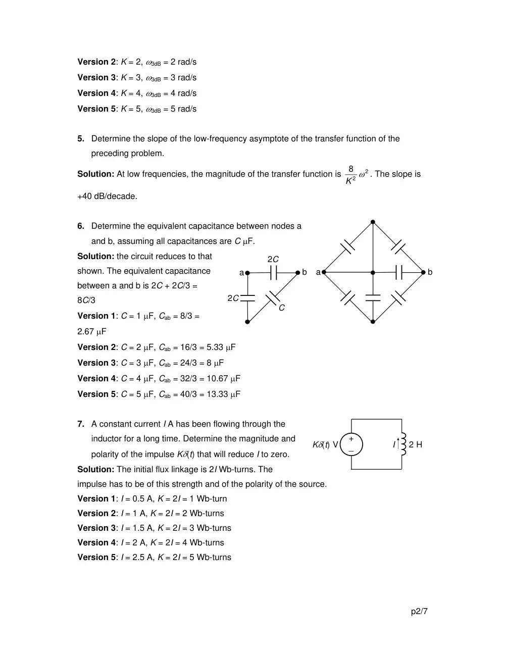
6. Determine the equivalent capacitance between nodes a
and b, assuming all capacitances are C μF.
Solution: the circuit reduces to that
shown. The equivalent capacitance
between a and b is 2C + 2C/3 =
8C/3
Version 1: C = 1 μF, Cab = 8/3 =
2.67 μF
Version 2: C = 2 μF, Cab = 16/3 = 5.33 μF
Version 3: C = 3 μF, Cab = 24/3 = 8 μF
Version 4: C = 4 μF, Cab = 32/3 = 10.67 μF
Version 5: C = 5 μF, Cab = 40/3 = 13.33 μF
7. A constant current I A has been flowing through the
inductor for a long time. Determine the magnitude and
polarity of the impulse Kδ(t) that will reduce I to zero.
Solution: The initial flux linkage is 2I Wb-turns. The
impulse has to be of this strength and of the polarity of the source.
Version 1: I = 0.5 A, K = 2I = 1 Wb-turn
Version 2: I = 1 A, K = 2I = 2 Wb-turns
Version 3: I = 1.5 A, K = 2I = 3 Wb-turns
Version 4: I = 2 A, K = 2I = 4 Wb-turns
Version 5: I = 2.5 A, K = 2I = 5 Wb-turns
a
b
a
b
2C
2C
C
_
+
2 H
Kδ(t) V
I
p3/7
v(t)
–
+
0.5 μF
i(t)
1.5 μF
2 μF
8. Evaluate the integral ∫
∞
∞
−
−
t dt
t e
K
t
cos( )
( )
2
δ
.
Solution: The integrand is zero everywhere except between 0- and 0+. Both
e 2t
− and cos(t)
are equal to 1 and are continuous at t = 0. The integral reduces to
K
t dt
K
=
∫
+
−
0
0
δ( )
.
Version 1: K = 2, integral = 2
Version 2: K = 3, integral = 3
Version 3: K = 4, integral = 4
Version 4: K = 5, integral = 5
Version 5: K = 6, integral = 6
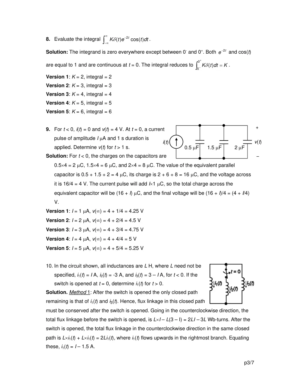
9. For t < 0, i(t) = 0 and v(t) = 4 V. At t = 0, a current
pulse of amplitude I μA and 1 s duration is
applied. Determine v(t) for t > 1 s.
Solution: For t < 0, the charges on the capacitors are
0.5×4 = 2 μC, 1.5×4 = 6 μC, and 2×4 = 8 μC. The value of the equivalent parallel
capacitor is 0.5 + 1.5 + 2 = 4 μC, its charge is 2 + 6 + 8 = 16 μC, and the voltage across
it is 16/4 = 4 V. The current pulse will add I×1 μC, so the total charge across the
equivalent capacitor will be (16 + I) μC, and the final voltage will be (16 + I)/4 = (4 + I/4)
V.
Version 1: I = 1 μA, v(∞) = 4 + 1/4 = 4.25 V
Version 2: I = 2 μA, v(∞) = 4 + 2/4 = 4.5 V
Version 3: I = 3 μA, v(∞) = 4 + 3/4 = 4.75 V
Version 4: I = 4 μA, v(∞) = 4 + 4/4 = 5 V
Version 5: I = 5 μA, v(∞) = 4 + 5/4 = 5.25 V
10. In the circuit shown, all inductances are L H, where L need not be
specified, i1(t) = I A, i2(t) = -3 A, and i3(t) = 3 – I A, for t < 0. If the
switch is opened at t = 0, determine i1(t) for t > 0.
Solution. Method 1: After the switch is opened the only closed path
remaining is that of i1(t) and i3(t). Hence, flux linkage in this closed path
must be conserved after the switch is opened. Going in the counterclockwise direction, the
total flux linkage before the switch is opened, is L×I – L(3 – I) = 2LI – 3L Wb-turns. After the
switch is opened, the total flux linkage in the counterclockwise direction in the same closed
path is L×i1(t) + L×i1(t) = 2Li1(t), where i1(t) flows upwards in the rightmost branch. Equating
these, i1(t) = I – 1.5 A.
p4/7
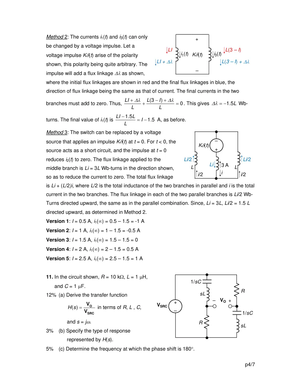
Method 2: The currents i1(t) and i3(t) can only
be changed by a voltage impulse. Let a
voltage impulse Kδ(t) arise of the polarity
shown, this polarity being quite arbitrary. The
impulse will add a flux linkage Δλ as shown,
where the initial flux linkages are shown in red and the final flux linkages in blue, the
direction of flux linkage being the same as that of current. The final currents in the two
branches must add to zero. Thus,
0
)
(3
=
+
−
+
+
L
I
L
L
LI
Δλ
Δλ
. This gives
Δλ = −1.5L
Wb-
turns. The final value of i1(t) is
1.5
1.5
−
=
−
I
L
L
LI
A, as before.
Method 3: The switch can be replaced by a voltage
source that applies an impulse Kδ(t) at t = 0. For t < 0, the
source acts as a short circuit, and the impulse at t = 0
reduces i2(t) to zero. The flux linkage applied to the
middle branch is Li = 3L Wb-turns in the direction shown,
so as to reduce the current to zero. The total flux linkage
is Li + (L/2)i, where L/2 is the total inductance of the two branches in parallel and i is the total
current in the two branches. The flux linkage in each of the two parallel branches is Li/2 Wb-
Turns directed upward, the same as in the parallel combination. Since, Li = 3L, Li/2 = 1.5 L
directed upward, as determined in Method 2.
Version 1: I = 0.5 A, i1(∞) = 0.5 – 1.5 = -1 A
Version 2: I = 1 A, i1(∞) = 1 – 1.5 = -0.5 A
Version 3: I = 1.5 A, i1(∞) = 1.5 – 1.5 = 0
Version 4: I = 2 A, i1(∞) = 2 – 1.5 = 0.5 A
Version 5: I = 2.5 A, i1(∞) = 2.5 – 1.5 = 1 A
11. In the circuit shown, R = 10 kΩ, L = 1 μH,
and C = 1 μF.
12% (a) Derive the transfer function
SRC
O
V
V
H(s) =
in terms of R, L , C,
and s = jω.
3% (b) Specify the type of response
represented by H(s).
5% (c) Determine the frequency at which the phase shift is 180°.
i1(t)
i3(t)
–
+
Kδ(t)
LI
L(3 – I)
LI + Δλ
L(3 – I) + Δλ
–
+
sL
–
VO +
VSRC
sL
1/sC
1/sC
R
R
3 A
Li/2
–
+
Kδ(t)
Li
L
L
i
i/2
i/2
Li/2
p5/7
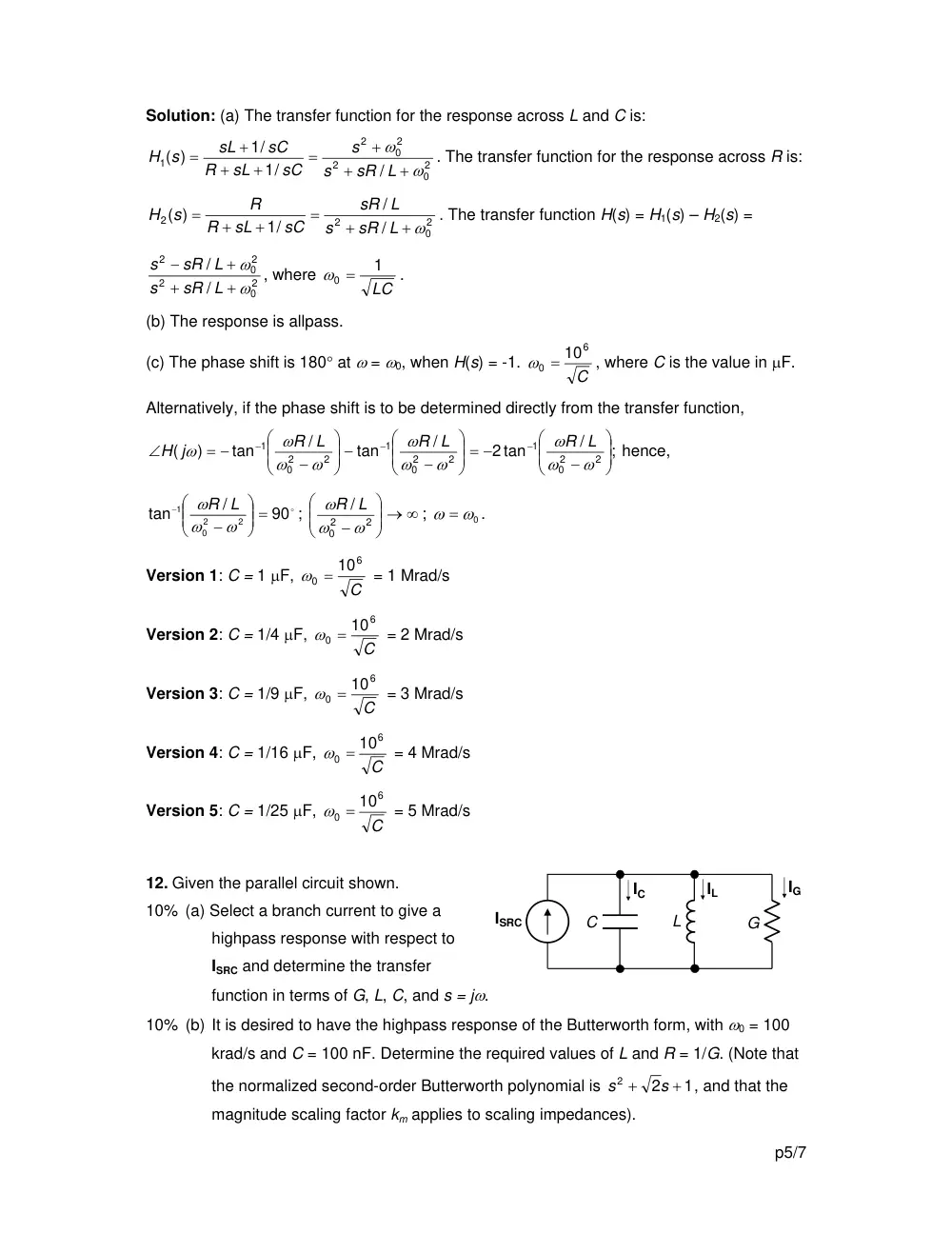
Solution: (a) The transfer function for the response across L and C is:
2
0
2
2
0
2
1
/
1/
1/
( )
ω
ω
+
+
+
=
+
+
+
=
sR L
s
s
sC
sL
R
sC
sL
H s
. The transfer function for the response across R is:
2
0
2
2
/
/
1/
( )
+ ω
+
=
+
+
=
sR L
s
sR L
sC
sL
R
R
s
H
. The transfer function H(s) = H1(s) – H2(s) =
2
0
2
2
0
2
/
/
ω
ω
+
+
+
−
sR L
s
sR L
s
, where
LC
1
ω0 =
.
(b) The response is allpass.
(c) The phase shift is 180° at ω = ω0, when H(s) = -1.
C
6
0
ω = 10
, where C is the value in μF.
Alternatively, if the phase shift is to be determined directly from the transfer function,
;
/
2 tan
/
tan
/
tan
)
(
2
2
0
1
2
2
0
1
2
2
0
1
⎟⎟
⎠
⎞
⎜⎜
⎝
⎛
−
⎟⎟ = −
⎠
⎞
⎜⎜
⎝
⎛
−
⎟⎟ −
⎠
⎞
⎜⎜
⎝
⎛
−
= −
∠
−
−
−
ω
ω
ω
ω
ω
ω
ω
ω
ω
ω
R L
R L
R L
H j
hence,
90o
/
tan
2
2
0
1
⎟⎟ =
⎠
⎞
⎜⎜
⎝
⎛
−
−
ω
ω
ω
R L
;
⎟⎟ → ∞
⎠
⎞
⎜⎜
⎝
⎛
−
2
2
0
/
ω
ω
ω
R L
;
ω = ω0
.
Version 1: C = 1 μF,
C
6
0
ω = 10
= 1 Mrad/s
Version 2: C = 1/4 μF,
C
6
0
= 10
ω
= 2 Mrad/s
Version 3: C = 1/9 μF,
C
6
0
= 10
ω
= 3 Mrad/s
Version 4: C = 1/16 μF,
C
6
0
ω = 10
= 4 Mrad/s
Version 5: C = 1/25 μF,
C
6
0
ω = 10
= 5 Mrad/s
12. Given the parallel circuit shown.
10% (a) Select a branch current to give a
highpass response with respect to
ISRC and determine the transfer
function in terms of G, L, C, and s = jω.
10% (b) It is desired to have the highpass response of the Butterworth form, with ω0 = 100
krad/s and C = 100 nF. Determine the required values of L and R = 1/G. (Note that
the normalized second-order Butterworth polynomial is
1
2
2
+
+
s
s
, and that the
magnitude scaling factor km applies to scaling impedances).
G
L
ISRC
IG
IL
IC
C
p6/7
Solution: (a) IC is zero at low frequencies and equals ISRC at infinite frequencies. It produces
a highpass response. The transfer function is
=
+
+
=
=
sL
sC
G
sC
H s
1/
)
(
SRC
C
I
I
2
0
0
2
2
2
2
)
/
(
1/
/
ω
ω
+
+
=
+
+
Q
s
s
s
LC
sG C
s
s
.
(b) For the required filter,
LC
1
ω0 =
,
C
L
2
0
1
ω
=
.
2
Q = 1
for a highpass Butterworth
response, scaled or not scaled. For the required filter
C
G
Q =
ω0
, so G =
ω0C 2
and R
=
2
1
ω0C
. If scaling is to be used, kf = ω0,
1
1
10 7
×
=
−
kmkf
,
0
7
1
10
kmω
=
−
,
0
10 7
1
− ω
km =
,
2
0
10 7
1
1
− ω
=
×
=
f
m
k
k
L
,
2
10
1
−7ω0
= G =
k
R
m
, where for the normalized Butterworth filter,
2
G =
, and km is uses as a scaling factor for R.
Version 1: ω0 = 100 krad/s,
1
10
10
1
1
7
10
2
0
≡
×
=
=
−
C
L
ω
mH,
=
=
2
1
0C
R
ω
50 2
2
100
2
10
10
1
7
5
=
=
×
−
Ω
Version 2: ω0 = 50 krad/s,
4
10
10
25
1
1
7
8
2
0
≡
×
×
=
=
−
C
L
ω
mH,
=
=
2
1
0C
R
ω
100 2
2
200
2
10
10
5
1
7
4
=
=
×
×
−
Ω
Version 3: ω0 = 40 krad/s,
≡
×
×
=
=
−7
8
2
0
10
10
16
1
1
C
L
ω
6.25 mH,
=
=
2
1
0C
R
ω
125 2
2
250
2
10
10
4
1
7
4
=
=
×
×
−
Ω
Version 4: ω0 = 25 krad/s,
≡
×
×
=
=
−7
8
2
0
10
10
6.25
1
1
C
L
ω
16 mH,
=
=
2
1
0C
R
ω
200 2
2
400
2
10
10
.5
2
1
7
4
=
=
×
×
−
Ω
Version 5: ω0 = 20 krad/s,
≡
×
×
=
=
−7
8
2
0
10
10
4
1
1
C
L
ω
25 mH,
=
=
2
1
0C
R
ω
250 2
2
500
2
10
10
2
1
7
4
=
=
×
×
−
Ω
13. The three capacitors are initially charged
as shown in the figure. The switch is
closed at t = 0. Determine:
8% (a) The value, voltage and charge on
the capacitor that is equivalent to
the three capacitors.
6% (b) The additional charge on this capacitor after the switch is closed.
2 μF
VSRC
4 μF
–
+
–
+
–
+
–
+
3 μF
15 μC
6 μC
12 μC
t = 0
–
+
V1
V2
p7/7
6% (c) The final values of V1 and V2. Check that V1 + V2 = VSRC.
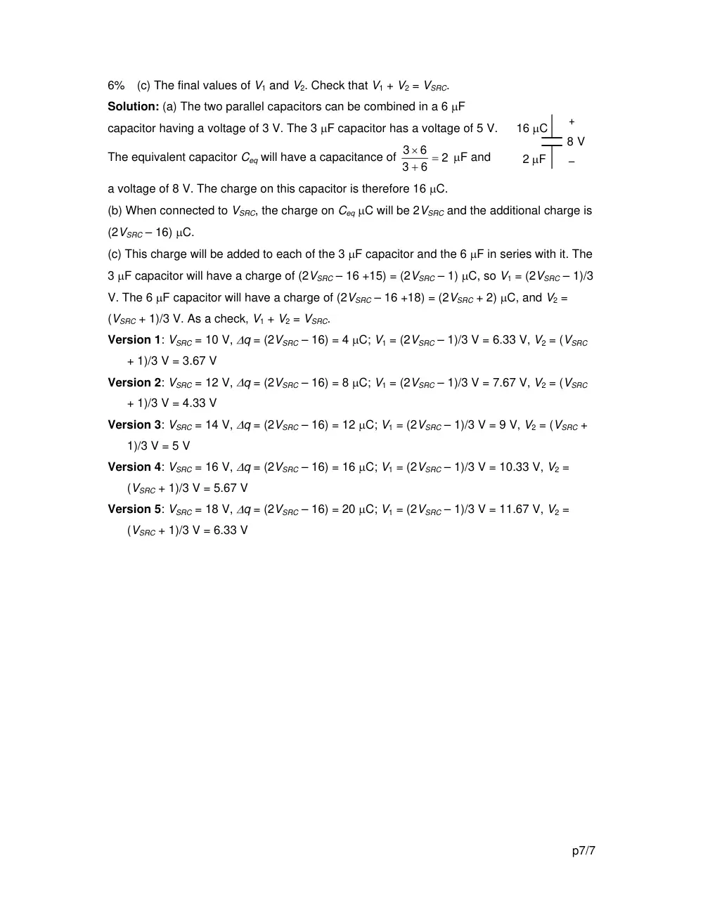
Solution: (a) The two parallel capacitors can be combined in a 6 μF
capacitor having a voltage of 3 V. The 3 μF capacitor has a voltage of 5 V.
The equivalent capacitor Ceq will have a capacitance of
2
6
3
6
3
=
+
×
μF and
a voltage of 8 V. The charge on this capacitor is therefore 16 μC.
(b) When connected to VSRC, the charge on Ceq μC will be 2VSRC and the additional charge is
(2VSRC – 16) μC.
(c) This charge will be added to each of the 3 μF capacitor and the 6 μF in series with it. The
3 μF capacitor will have a charge of (2VSRC – 16 +15) = (2VSRC – 1) μC, so V1 = (2VSRC – 1)/3
V. The 6 μF capacitor will have a charge of (2VSRC – 16 +18) = (2VSRC + 2) μC, and V2 =
(VSRC + 1)/3 V. As a check, V1 + V2 = VSRC.
Version 1: VSRC = 10 V, Δq = (2VSRC – 16) = 4 μC; V1 = (2VSRC – 1)/3 V = 6.33 V, V2 = (VSRC
+ 1)/3 V = 3.67 V
Version 2: VSRC = 12 V, Δq = (2VSRC – 16) = 8 μC; V1 = (2VSRC – 1)/3 V = 7.67 V, V2 = (VSRC
+ 1)/3 V = 4.33 V
Version 3: VSRC = 14 V, Δq = (2VSRC – 16) = 12 μC; V1 = (2VSRC – 1)/3 V = 9 V, V2 = (VSRC +
1)/3 V = 5 V
Version 4: VSRC = 16 V, Δq = (2VSRC – 16) = 16 μC; V1 = (2VSRC – 1)/3 V = 10.33 V, V2 =
(VSRC + 1)/3 V = 5.67 V
Version 5: VSRC = 18 V, Δq = (2VSRC – 16) = 20 μC; V1 = (2VSRC – 1)/3 V = 11.67 V, V2 =
(VSRC + 1)/3 V = 6.33 V
–
+
8 V
2 μF
16 μC