
EECE 310 Final with Answers, Fall 2015
American University of Beirut · Electronics · 8 pages · with solution


More EECE 310 files
- Final 30 Questions No Answers · Fall 2011Final exam · with solutionView
- Lecture Slides of Chapter 15 · Summer 2019LabView
- Lecture Slides of Chapter 16 · Summer 2019LabView
- Lecture Slides of Chapter 14 · Summer 2019LabView
- Lecture Slides of Chapter 13 · Summer 2019LabView
- Lecture Slides of Chapter 17 · Summer 2019LabView
- Lecture Slides of Chapter 11 · Summer 2019LabView
- Lecture Slides of Chapter 12 · Summer 2019LabView
Show the text of this final exam
EECE 310 – Final Exam – Fall 2015 – Page 1 of 8
American University of Beirut
Department of Electrical and Computer Engineering
EECE 310 Electronics Final Exam - Closed Book
2 hours (120 minutes)
December 18, 2015
ALL QUESTIONS ARE GRADED EQUALLY
PENALTY IS 5 TO 1
NAME______ ____________________ID number__ ______________ signature here
SIGN: I HAVE NEITHER GIVEN NOR RECEIVED AID ON THIS EXAM
v
v
v There are 8 pages and 25 problems
v
v
v Unless otherwise specified, assume that:
• VT = 25 mV
• |VBE(ACTIVE)| = 0.7 V
• |VBE(SAT)| = 0.7 V
• |VCE(SAT)| = 0.2 V
• |VCE(EDGE OF SAT)| = 0.3 V
•
• All capacitors are very large
•
• Base-width modulation (Early effect) and channel-length modulation
effects are negligible
EECE 310 – Final Exam – Fall 2015 – Page 2 of 8
1. In the circuit shown below, the diode is ideal. At what value of VA (in V) does the
diode start to conduct? Assume that RA = 22 kΩ, VB = 16 V, and RB = 10 kΩ.
a) 35.2
b) 30.8
c) 26.4
d) 39.6
e) 44.0
2. Find the current in RA (in mA) when VA = 10 V.
a) 0.750
b) 0.813
c) 0.875
d) 0.938
e) 0.688
3. In the circuit shown below, the diode drops 0.7 V when conducting, and is
considered an open-circuit when OFF. Find the maximum diode current (in mA) if vS
is a square wave that varies between +20 V (for 50% of the time) and –20 V (for the
other 50% of the time). Assume VA = 8 V and R = 2.2 kΩ.
a) 2.86
b) 5.14
c) 4.23
d) 3.77
e) 3.32
4. In the previous problem, find the average value of the output voltage vO (in V).
a) –3.65
b) –3.15
c) –5.65
d) –4.65
e) –4.15
5. A series connection of 10 identical PN junction diodes in the same polarity, also
connected in series with a battery such that all diodes are forward biased, results in a
forward current of 1 mA when the battery voltage is 7 V, and 6 mA when the battery
voltage is 7.5 V. Find the value of n for the diodes.
a) 1.820
b) 1.116
c) 1.243
d) 1.443
e) 1.028
VA
VB
+
+
RA
RB
VA
+
R
vS
+
+
_
vO
EECE 310 – Final Exam – Fall 2015 – Page 3 of 8
6. Consider the Zener diode in the circuit shown below. The diode has VZ0 = 12.0 V,
rZ = 100 W, and IZK = 5 mA. Find the output voltage vO (in V) when vS is 35.0 V?
a) 10.0
b) 11.0
c) 11.5
d) 11.7
e) 11.9
7. A logic inverter has NML = NMH = 0.5 V, VOL = 0.4 V, and VOH = 3.5 V. Find the
value of VIL for this inverter (in V).
a) 0.9
b) 1.0
c) 0.7
d) 0.8
e) 0.6
The drain current of an enhancement NMOS is measured at several values of VGS and
VDS, as shown in the table below. For this MOSFET: 𝑘"
# $
% = 1 mA/V2, 𝑉* = 1 V, and
𝜆 ≠ 0. Answer the following 2 questions.
VGS [V]
VDS [V]
ID [mA]
3
3
2.06
3
8
ID1
3
0.2
ID2
8. Find the value of ID1 (in mA).
a) 2.48
b) 2.16
c) 2.24
d) 2.32
e) 2.40
9. Find the value of ID2 (in mA).
a) 0.38
b) 0.72
c) 1.02
d) 1.28
e) 1.5
=+
vS
2k⌦
5k⌦
+
_
vO
EECE 310 – Final Exam – Fall 2015 – Page 4 of 8
The enhancement NMOS in the circuit shown below has 𝑘"
# $
% = 2 mA/V2, 𝑉* = 1 V,
and 𝜆 = 0. RD = 6 kΩ and the MOSFET operates at the boundary between the triode
and saturation regions. Answer the following 2 questions.
10. Find the value of the drain current ID (in mA).
a) 2.5
b) 7.5
c) 5
d) 3.75
e) 3
11. Find the value of RS (in kΩ).
a) 3.76
b) 4.57
c) 1.37
d) 2.15
e) 2.95
12. The enhancement PMOS in the circuit shown has 𝑘/
# $
% = 2 mA/V2, 𝑉* = −1.5 V,
and 𝜆 = 0. Find VDS (in V) if RD = RS, and the MOSFET is biased such that
VGS = –3.5 V.
a) –15
b) –16
c) –17
d) –19
e) –18
13. A voltage amplifier has an open-circuit voltage gain of 100 V/V, an output
resistance of 100 Ω, and a power gain of 150×106 W/W when a 100 Ω load is
connected across the output terminals. Find the input resistance (in MΩ).
a) 6
b) 5
c) 2
d) 3
e) 4
EECE 310 – Final Exam – Fall 2015 – Page 5 of 8
14. The enhancement NMOS in the circuit shown below is biased in the saturation
region such that the gate to source overdrive voltage VOV is 0.5 V and the drain
current ID = 1 mA. If vs is a 60 mV peak-to-peak sinusoid, find the peak-to-peak
variation of vo (in mV). Assume that 𝜆 = 0.
a) 36.0
b) 43.2
c) 50.4
d) 21.6
e) 28.8
The enhancement NMOS in the circuit shown below has an early voltage VA = 75 V;
it is biased in the saturation region such that ID = 1 mA and VDS = 5 V. vi is a signal
voltage. Answer the following 2 questions.
15. If Rout = 10 kΩ, find the value of RD (in kΩ).
a) 25.71
b) 9.23
c) 12
d) 18.26
e) 21.82
16. If RD = 20 kΩ and the MOSFET transconductance gm = 1.2 mA/V, find the small-
signal voltage gain vo/vi (in V/V); vo is the signal component of the total output
voltage vO.
a) –23.94
b) –17.94
c) –20.94
d) –26.94
e) –14.94
EECE 310 – Final Exam – Fall 2015 – Page 6 of 8
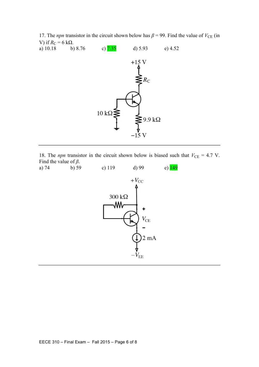
17. The npn transistor in the circuit shown below has β = 99. Find the value of VCE (in
V) if RC = 6 kΩ.
a) 10.18
b) 8.76
c) 7.35
d) 5.93
e) 4.52
18. The npn transistor in the circuit shown below is biased such that VCE = 4.7 V.
Find the value of β.
a) 74
b) 59
c) 119
d) 99
e) 149
EECE 310 – Final Exam – Fall 2015 – Page 7 of 8
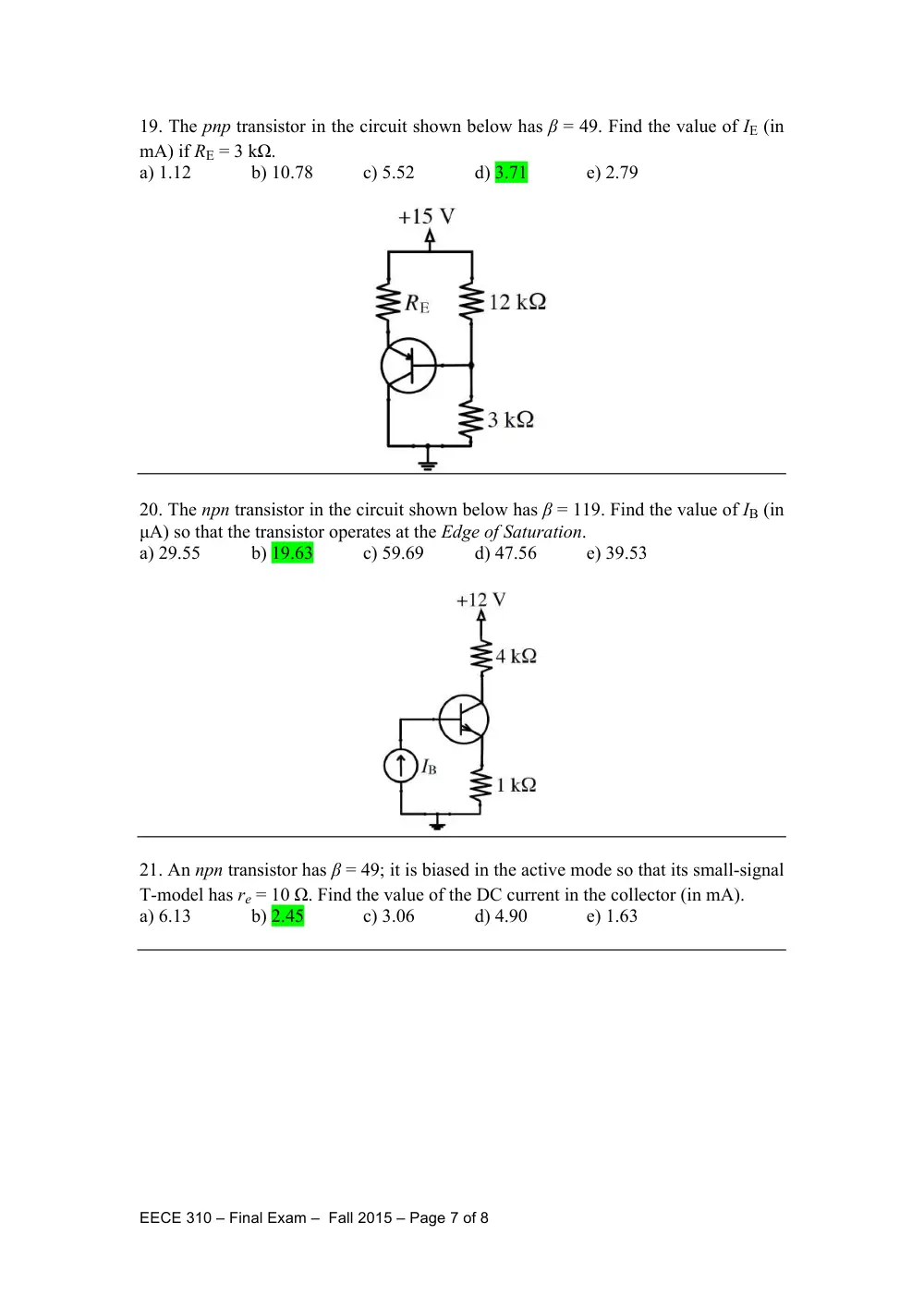
19. The pnp transistor in the circuit shown below has β = 49. Find the value of IE (in
mA) if RE = 3 kΩ.
a) 1.12
b) 10.78
c) 5.52
d) 3.71
e) 2.79
20. The npn transistor in the circuit shown below has β = 119. Find the value of IB (in
µA) so that the transistor operates at the Edge of Saturation.
a) 29.55
b) 19.63
c) 59.69
d) 47.56
e) 39.53
21. An npn transistor has β = 49; it is biased in the active mode so that its small-signal
T-model has re = 10 Ω. Find the value of the DC current in the collector (in mA).
a) 6.13
b) 2.45
c) 3.06
d) 4.90
e) 1.63
EECE 310 – Final Exam – Fall 2015 – Page 8 of 8
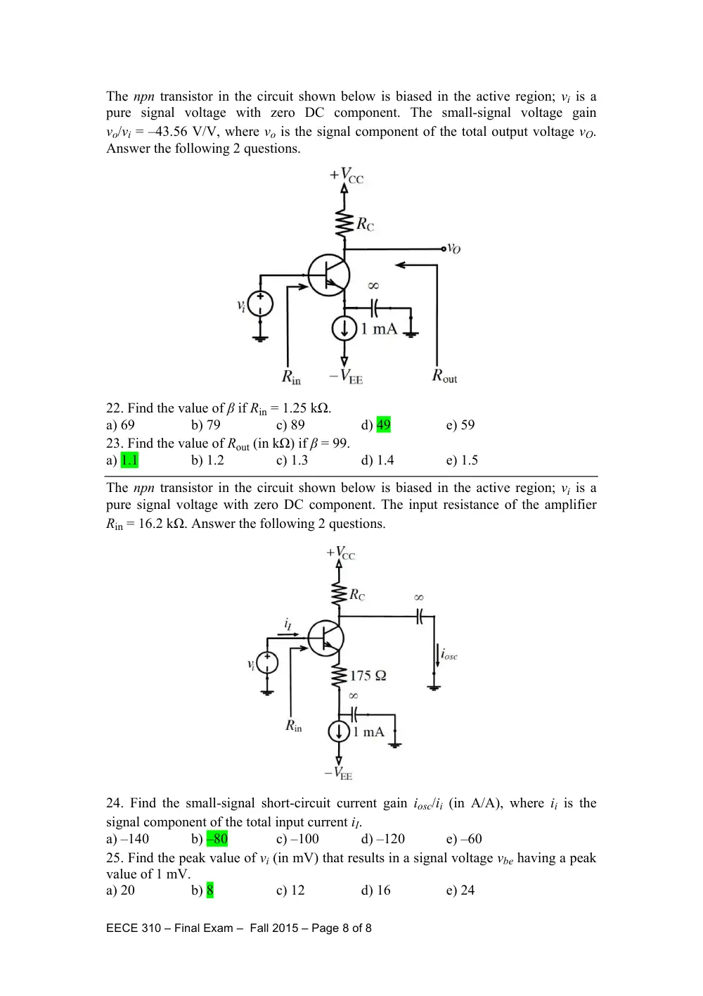
The npn transistor in the circuit shown below is biased in the active region; vi is a
pure signal voltage with zero DC component. The small-signal voltage gain
vo/vi = –43.56 V/V, where vo is the signal component of the total output voltage vO.
Answer the following 2 questions.
22. Find the value of β if Rin = 1.25 kΩ.
a) 69
b) 79
c) 89
d) 49
e) 59
23. Find the value of Rout (in kΩ) if β = 99.
a) 1.1
b) 1.2
c) 1.3
d) 1.4
e) 1.5
The npn transistor in the circuit shown below is biased in the active region; vi is a
pure signal voltage with zero DC component. The input resistance of the amplifier
Rin = 16.2 kΩ. Answer the following 2 questions.
24. Find the small-signal short-circuit current gain iosc/ii (in A/A), where ii is the
signal component of the total input current iI.
a) –140
b) –80
c) –100
d) –120
e) –60
25. Find the peak value of vi (in mV) that results in a signal voltage vbe having a peak
value of 1 mV.
a) 20
b) 8
c) 12
d) 16
e) 24