
EECE 311 Final Solutions, Spring 2013
American University of Beirut · Electronic Circuits · 6 pages · Prof. Ayman Kayssi · with solution

More EECE 311 files
- Final 2010 · Spring 2013Final examView
- Final · Spring 2013Final examView
- Final with Solutions · Spring 2010Final exam · with solutionView
- Final · Fall 2003Final examView
- Useful File Summary for Some Components · Summer 2018FileView
- Useful File Summary for Some Components · Summer 2018FileView
- Midterm with Answers · Spring 2014Exam · with solutionView
- Homework All Hw 2013+midterm · Spring 2013ExamView
Show the text of this final exam
EECE 311 – Final Exam – Spring 2013 – Page 1 of 6
American University of Beirut
Department of Electrical and Computer Engineering
EECE 311 – Electronic Circuits
Spring 2013
Final Exam – May 23, 2013
Open Book – 120 minutes
NAME:___________________________ ID Number: ______________________
o Mark all your answers and ID number on the computer (Scantron) sheet.
o All problems are graded equally.
o There are 6 pages and 25 problems.
o Penalty is 5-to-1 (one to four wrong answers do not cancel a correct answer.)
EECE 311 – Final Exam – Spring 2013 – Page 2 of 6
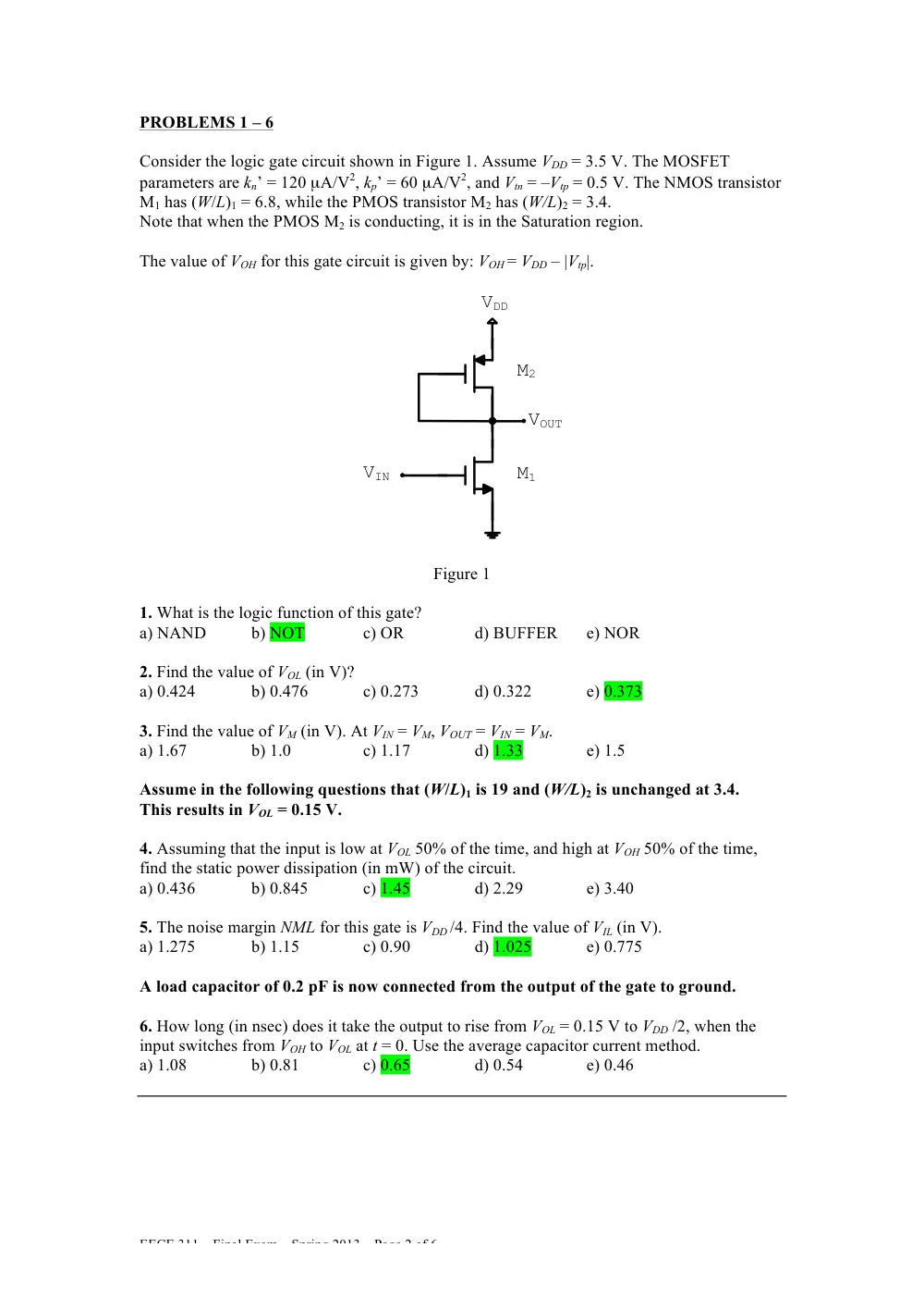
PROBLEMS 1 – 6
Consider the logic gate circuit shown in Figure 1. Assume VDD = 3.5 V. The MOSFET
parameters are kn’ = 120 µA/V2, kp’ = 60 µA/V2, and Vtn = –Vtp = 0.5 V. The NMOS transistor
M1 has (W/L)1 = 6.8, while the PMOS transistor M2 has (W/L)2 = 3.4.
Note that when the PMOS M2 is conducting, it is in the Saturation region.
The value of VOH for this gate circuit is given by: VOH = VDD – |Vtp|.
VDD
VOUT
VIN
M2
M1
Figure 1
1. What is the logic function of this gate?
a) NAND
b) NOT
c) OR
d) BUFFER
e) NOR
2. Find the value of VOL (in V)?
a) 0.424
b) 0.476
c) 0.273
d) 0.322
e) 0.373
3. Find the value of VM (in V). At VIN = VM, VOUT = VIN = VM.
a) 1.67
b) 1.0
c) 1.17
d) 1.33
e) 1.5
Assume in the following questions that (W/L)1 is 19 and (W/L)2 is unchanged at 3.4.
This results in VOL = 0.15 V.
4. Assuming that the input is low at VOL 50% of the time, and high at VOH 50% of the time,
find the static power dissipation (in mW) of the circuit.
a) 0.436
b) 0.845
c) 1.45
d) 2.29
e) 3.40
5. The noise margin NML for this gate is VDD /4. Find the value of VIL (in V).
a) 1.275
b) 1.15
c) 0.90
d) 1.025
e) 0.775
A load capacitor of 0.2 pF is now connected from the output of the gate to ground.
6. How long (in nsec) does it take the output to rise from VOL = 0.15 V to VDD /2, when the
input switches from VOH to VOL at t = 0. Use the average capacitor current method.
a) 1.08
b) 0.81
c) 0.65
d) 0.54
e) 0.46
EECE 311 – Final Exam – Spring 2013 – Page 3 of 6
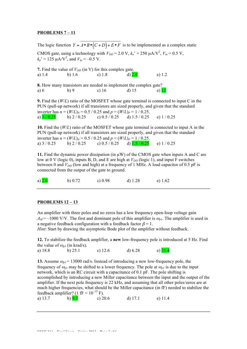
PROBLEMS 7 – 11
The logic function Y = A•B• C + D
(
)+ E •F is to be implemented as a complex static
CMOS gate, using a technology with VDD = 2.0 V, kn’ = 250 µA/V2, Vtn = 0.5 V,
kp’ = 125 µA/V2, and Vtp = –0.5 V.
7. Find the value of VOH (in V) for this complex gate.
a) 1.4
b) 1.6
c) 1.8
d) 2.0
e) 1.2
8. How many transistors are needed to implement the complex gate?
a) 6
b) 9
c) 16
d) 15
e) 12
9. Find the (W/L) ratio of the MOSFET whose gate terminal is connected to input C in the
PUN (pull-up network) if all transistors are sized properly, and given that the standard
inverter has n = (W/L)N = 0.5 / 0.25 and p = (W/L)P = 1 / 0.25.
a) 3 / 0.25
b) 2 / 0.25
c) 0.5 / 0.25
d) 1.5 / 0.25
e) 1 / 0.25
10. Find the (W/L) ratio of the MOSFET whose gate terminal is connected to input A in the
PUN (pull-up network) if all transistors are sized properly, and given that the standard
inverter has n = (W/L)N = 0.5 / 0.25 and p = (W/L)P = 1 / 0.25.
a) 3 / 0.25
b) 2 / 0.25
c) 0.5 / 0.25
d) 1.5 / 0.25
e) 1 / 0.25
11. Find the dynamic power dissipation (in µW) of the CMOS gate when inputs A and C are
low at 0 V (logic 0), inputs B, D, and E are high at VDD (logic 1), and input F switches
between 0 and VDD (low and high) at a frequency of 1 MHz. A load capacitor of 0.5 pF is
connected from the output of the gate to ground.
a) 2.0
b) 0.72
c) 0.98
d) 1.28
e) 1.62
PROBLEMS 12 – 13
An amplifier with three poles and no zeros has a low frequency open-loop voltage gain
AM = –1000 V/V. The first and dominant pole of this amplifier is ωp1. The amplifier is used in
a negative feedback configuration with a feedback factor β = 1.
Hint: Start by drawing the asymptotic Bode plot of the amplifier without feedback.
12. To stabilize the feedback amplifier, a new low-frequency pole is introduced at 5 Hz. Find
the value of ωp1 (in krad/s).
a) 18.8
b) 25.1
c) 12.6
d) 6.28
e) 31.4
13. Assume ωp1 = 13000 rad/s. Instead of introducing a new low-frequency pole, the
frequency of ωp1 may be shifted to a lower frequency. The pole at ωp1 is due to the input
network, which is an RC circuit with a capacitance of 0.1 pF. The pole shifting is
accomplished by introducing a new Miller capacitance between the input and the output of the
amplifier. If the next pole frequency is 22 kHz, and assuming that all other poles/zeros are at
much higher frequencies, what should be the Miller capacitance (in fF) needed to stabilize the
feedback amplifier? (1 fF = 10–15 F).
a) 13.7
b) 9.3
c) 20.6
d) 17.1
e) 11.4
EECE 311 – Final Exam – Spring 2013 – Page 4 of 6
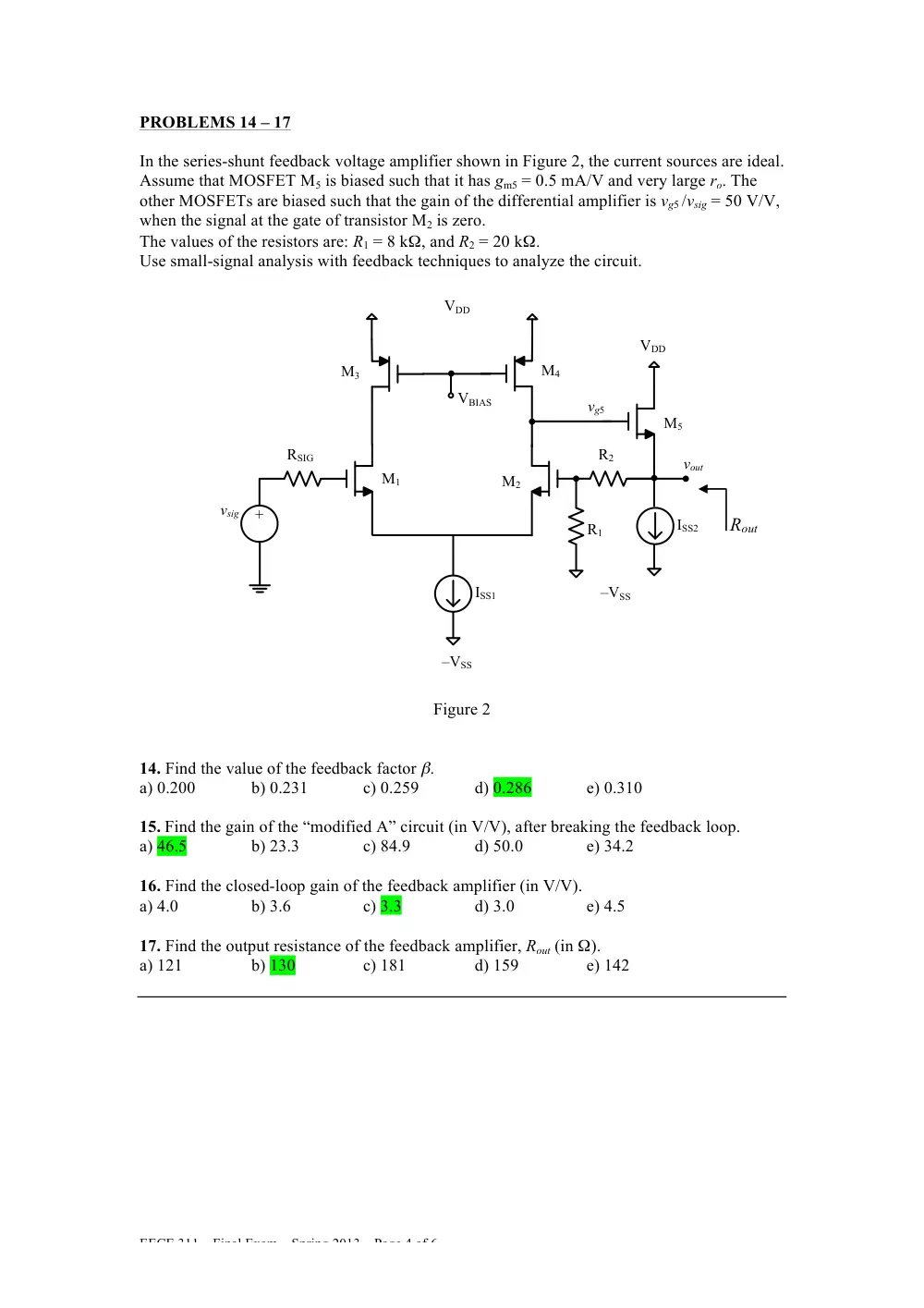
PROBLEMS 14 – 17
In the series-shunt feedback voltage amplifier shown in Figure 2, the current sources are ideal.
Assume that MOSFET M5 is biased such that it has gm5 = 0.5 mA/V and very large ro. The
other MOSFETs are biased such that the gain of the differential amplifier is vg5 /vsig = 50 V/V,
when the signal at the gate of transistor M2 is zero.
The values of the resistors are: R1 = 8 kΩ, and R2 = 20 kΩ.
Use small-signal analysis with feedback techniques to analyze the circuit.
VDD
vsig
M4
VBIAS
M3
M1
M2
ISS1
M5
VDD
–VSS
–VSS
RSIG
R1
+
vout
R2
ISS2
vg5
Figure 2
14. Find the value of the feedback factor β.
a) 0.200
b) 0.231
c) 0.259
d) 0.286
e) 0.310
15. Find the gain of the “modified A” circuit (in V/V), after breaking the feedback loop.
a) 46.5
b) 23.3
c) 84.9
d) 50.0
e) 34.2
16. Find the closed-loop gain of the feedback amplifier (in V/V).
a) 4.0
b) 3.6
c) 3.3
d) 3.0
e) 4.5
17. Find the output resistance of the feedback amplifier, Rout (in Ω).
a) 121
b) 130
c) 181
d) 159
e) 142
Rout
EECE 311 – Final Exam – Spring 2013 – Page 5 of 6
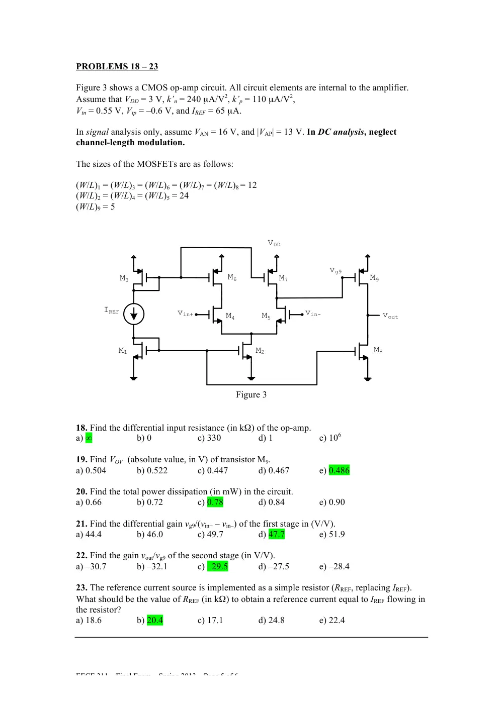
PROBLEMS 18 – 23
Figure 3 shows a CMOS op-amp circuit. All circuit elements are internal to the amplifier.
Assume that VDD = 3 V, k’n = 240 µA/V2, k’p = 110 µA/V2,
Vtn = 0.55 V, Vtp = –0.6 V, and IREF = 65 µA.
In signal analysis only, assume VAN = 16 V, and |VAP| = 13 V. In DC analysis, neglect
channel-length modulation.
The sizes of the MOSFETs are as follows:
(W/L)1 = (W/L)3 = (W/L)6 = (W/L)7 = (W/L)8 = 12
(W/L)2 = (W/L)4 = (W/L)5 = 24
(W/L)9 = 5
IREF
M1
M3
VDD
M2
vin+
vin-
M4
M5
M6
M7
M9
M8
vout
vg9
Figure 3
18. Find the differential input resistance (in kΩ) of the op-amp.
a) ∞
b) 0
c) 330
d) 1
e) 106
19. Find VOV (absolute value, in V) of transistor M9.
a) 0.504
b) 0.522
c) 0.447
d) 0.467
e) 0.486
20. Find the total power dissipation (in mW) in the circuit.
a) 0.66
b) 0.72
c) 0.78
d) 0.84
e) 0.90
21. Find the differential gain vg9/(vin+ – vin–) of the first stage in (V/V).
a) 44.4
b) 46.0
c) 49.7
d) 47.7
e) 51.9
22. Find the gain vout/vg9 of the second stage (in V/V).
a) –30.7
b) –32.1
c) –29.5
d) –27.5
e) –28.4
23. The reference current source is implemented as a simple resistor (RREF, replacing IREF).
What should be the value of RREF (in kΩ) to obtain a reference current equal to IREF flowing in
the resistor?
a) 18.6
b) 20.4
c) 17.1
d) 24.8
e) 22.4
EECE 311 – Final Exam – Spring 2013 – Page 6 of 6
PROBLEMS 24 – 25
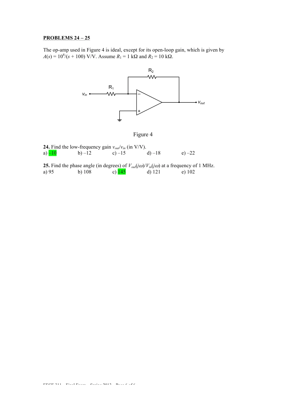
The op-amp used in Figure 4 is ideal, except for its open-loop gain, which is given by
A(s) = 108/(s + 100) V/V. Assume R1 = 1 kΩ and R2 = 10 kΩ.
–
+
R2
R1
vout
vin
Figure 4
24. Find the low-frequency gain vout/vin (in V/V).
a) –10
b) –12
c) –15
d) –18
e) –22
25. Find the phase angle (in degrees) of Vout(jω)/Vin(jω) at a frequency of 1 MHz.
a) 95
b) 108
c) 145
d) 121
e) 102