
EECE 311 Homework, Spring 2008
American University of Beirut · Electronic Circuits · 3 pages

More EECE 311 files
- Homework 1 · Spring 2012HomeworkView
- Homework All Hws + Solutions (sping 2012) · Spring 2012Homework · with solutionView
- Homework · Spring 2008HomeworkView
- Homework · Spring 2008HomeworkView
- Homework · Spring 2008HomeworkView
- Homework · Spring 2008HomeworkView
- Homework · Spring 2008HomeworkView
- Homework · Spring 2008HomeworkView
Show the text of this homework
American University of Beirut
DEPARTMENT OF ELECTRICAL AND COMPUTER ENGINEERING
EECE 311 – Electronic Circuits (Sections 1 & 2)
Spring 2008
HOMEWORK 2
Due Wednesday March 12, 2008 at 1:00 PM
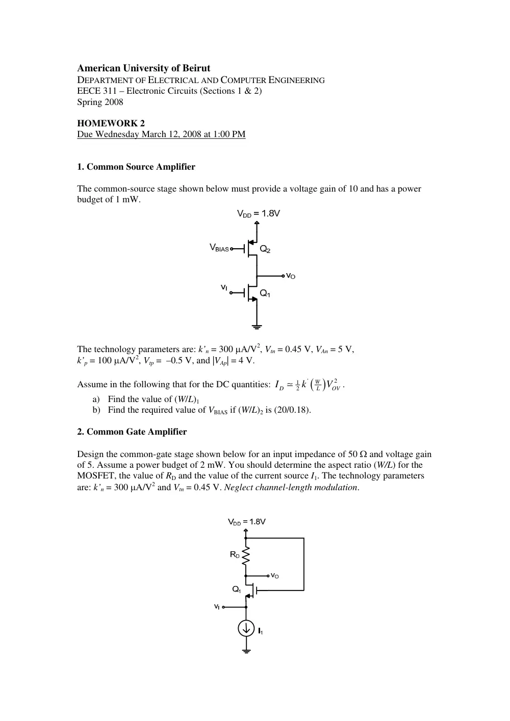
1. Common Source Amplifier
The common-source stage shown below must provide a voltage gain of 10 and has a power
budget of 1 mW.
The technology parameters are: k’n = 300 μA/V2, Vtn = 0.45 V, VAn = 5 V,
k’p = 100 μA/V2, Vtp = –0.5 V, and |VAp| = 4 V.
Assume in the following that for the DC quantities:
( )
'
2
1
2
W
D
OV
L
I
k
V
�
.
a) Find the value of (W/L)1
b) Find the required value of VBIAS if (W/L)2 is (20/0.18).
2. Common Gate Amplifier
Design the common-gate stage shown below for an input impedance of 50 Ω and voltage gain
of 5. Assume a power budget of 2 mW. You should determine the aspect ratio (W/L) for the
MOSFET, the value of RD and the value of the current source I1. The technology parameters
are: k’n = 300 μA/V2 and Vtn = 0.45 V. Neglect channel-length modulation.
3. Emitter Follower
Design the emitter-follower circuit shown below for a power budget of 3 mW and an output
impedance of 50 Ω. Neglect base width modulation, and assume that β → ∞ . Determine that
value of IREF and the value of the ratio AE1/AE-REF.
4. MOSFET Cascode
For the cascode circuit shown below, assume (W/L) = 10 μm/0.18 μm for all MOSFETs, and
that VBIAS = 0.9 V. Use PSpice to plot the input-output characteristics (vo versus vi). Note that
the body terminals are connected to the supplies (ground for NMOS and VDD for PMOS.)
Determine from the plot the point at which the small-signal gain is maximum, in absolute
value.
Now suppose the biasing circuitry that produces the above DC value of vI incurs an error of
+/– 20 mV. Explain what happens to the voltage gain.
Use the SPICE models posted on Moodle.
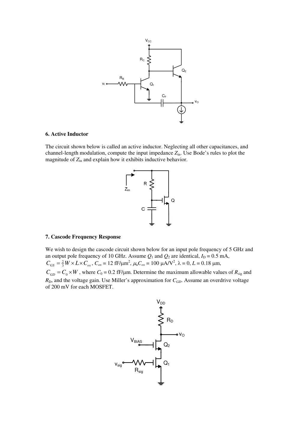
5. Miller’s Theorem
Use Miller’s theorem to estimate the input and output poles of the circuit shown below.
Neglect base-width modulation and the internal BJT capacitors.
vI
VCC
vO
Q1
Q2
CF
RB
RC
6. Active Inductor
The circuit shown below is called an active inductor. Neglecting all other capacitances, and
channel-length modulation, compute the input impedance Zin. Use Bode’s rules to plot the
magnitude of Zin and explain how it exhibits inductive behavior.
7. Cascode Frequency Response
We wish to design the cascode circuit shown below for an input pole frequency of 5 GHz and
an output pole frequency of 10 GHz. Assume Q1 and Q2 are identical, ID = 0.5 mA,
2
3
GS
ox
C
W
L C
=
×
×
, Cox = 12 fF/μm2, μnCox = 100 μA/V2, λ = 0, L = 0.18 μm,
0
CGD
C
W
=
×
, where C0 = 0.2 fF/μm. Determine the maximum allowable values of Rsig and
RD, and the voltage gain. Use Miller’s approximation for CGD. Assume an overdrive voltage
of 200 mV for each MOSFET.
vsig
Q1
vO
Q2
VBIAS
Rsig
RD
VDD