
EECE 311 Midterm, Fall 2010
American University of Beirut · Electronic Circuits · 58 pages


Showing the first 10 of 58 pages. Download the PDF to see all of it.
More EECE 311 files
- Midterm with Answers · Spring 2014Exam · with solutionView
- Homework All Hw 2013+midterm · Spring 2013ExamView
- Midterm with Answers · Spring 2011Exam · with solutionView
- Midterm · Summer 2010ExamView
- Exam 1 · Spring 2008ExamView
- Exam 1 · Spring 2008ExamView
- Exam 2 · Spring 2008ExamView
- Exam 2 · Spring 2008ExamView
Show the text of this exam
American University of Beirut
Faculty of Engineering and Architecture
Department of Electrical and Computer Engineering
EE 042 - Analog Electronics
Instructors: A. Kayssi and M. Krisht
Quiz 1
Saturday November 23, 1996
Closed Book
Programmable Calculators Are Not Allowed.
Time: 1.5 hours
VERSION A
The figures for this quiz are missing
Name:_______________________________ ID#:__________________________
! Provide your answer on the computer card only.
! Return the computer card attached to the question sheet.
! Use a pencil for marking your answers and ID number on the computer card.
! When using an eraser, make sure you erased well.
! On this sheet, write with a pen your name followed by your ID number.
! All questions are graded equally.
1. What is the version of your question sheet? (This question is not graded.)
a) Version A
b) Version B
c) Version C
d) Version D
e) Version E
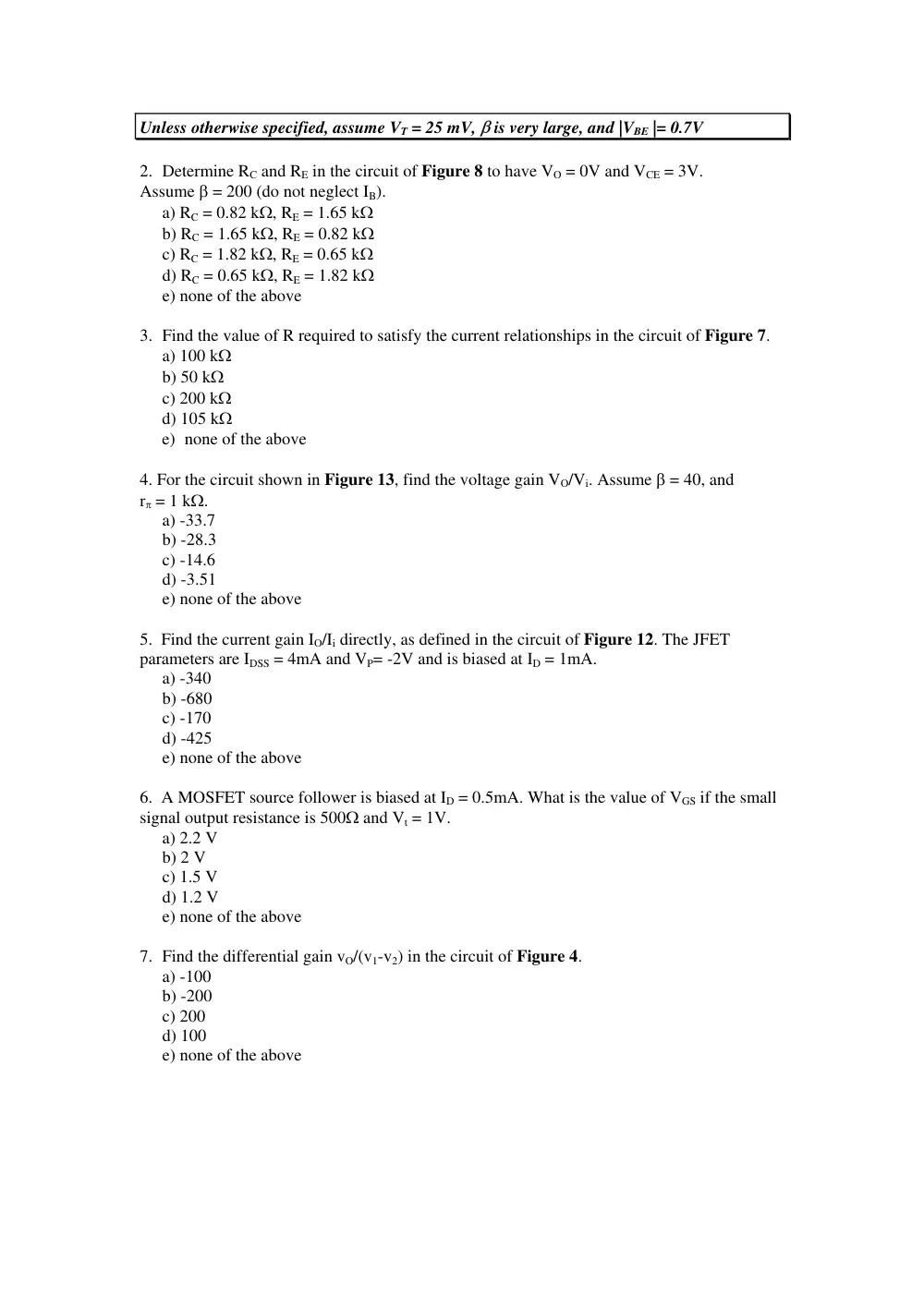
Unless otherwise specified, assume VT = 25 mV, β is very large, and |VBE |= 0.7V
2. Determine RC and RE in the circuit of Figure 8 to have VO = 0V and VCE = 3V.
Assume β = 200 (do not neglect IB).
a) RC = 0.82 kΩ, RE = 1.65 kΩ
b) RC = 1.65 kΩ, RE = 0.82 kΩ
c) RC = 1.82 kΩ, RE = 0.65 kΩ
d) RC = 0.65 kΩ, RE = 1.82 kΩ
e) none of the above
3. Find the value of R required to satisfy the current relationships in the circuit of Figure 7.
a) 100 kΩ
b) 50 kΩ
c) 200 kΩ
d) 105 kΩ
e) none of the above
4. For the circuit shown in Figure 13, find the voltage gain VO/Vi. Assume β = 40, and
rπ = 1 kΩ.
a) -33.7
b) -28.3
c) -14.6
d) -3.51
e) none of the above
5. Find the current gain IO/Ii directly, as defined in the circuit of Figure 12. The JFET
parameters are IDSS = 4mA and VP= -2V and is biased at ID = 1mA.
a) -340
b) -680
c) -170
d) -425
e) none of the above
6. A MOSFET source follower is biased at ID = 0.5mA. What is the value of VGS if the small
signal output resistance is 500Ω and Vt = 1V.
a) 2.2 V
b) 2 V
c) 1.5 V
d) 1.2 V
e) none of the above
7. Find the differential gain vO/(v1-v2) in the circuit of Figure 4.
a) -100
b) -200
c) 200
d) 100
e) none of the above
8. Find the common-mode rejection ratio (CMRR) for the circuit of Figure 4.
Assume VA = 100V.
a) 73 dB
b) 82 dB
c) 66 dB
d) 78 dB
e) none of the above
9. Find the value of the emitter resistors, to be inserted between the emitters of Q1 and Q2 and
node X in the circuit of Figure 4, to have a differential input resistance of 200KΩ. Assume β
= 99.
a) 1.5 kΩ
b) 5 kΩ
c) 150 Ω
d) 35 Ω
e) none of the above
10. Find the value of R in the circuit of Figure 3 in order to have VO = 2V.
a) 7.17 kΩ
b) 9.5 kΩ
c) 14.3 kΩ
d) 19 kΩ
e) none of the above
11. All the BJTs in the circuit of Figure 9 are biased at IC=1mA and have β = 100. Find VO/V3
and V3/V2. (Hint: Include the loading effect of the last stage on the second stage).
a) VO/V3 = -60 ,V3/V2 = 0.985
b) VO/V3 = -80 ,V3/V2 = 0.994
c) VO/V3 = -60 ,V3/V2 = 0.994
d) VO/V3 = -80 ,V3/V2 = 0.985
e) none of the above
12. Find VO/VS in the circuit of Figure 9.
a) 540.5
b) 187.4
c) 932.6
d) 349.1
e) none of the above
13. Find the range of values of IO in the circuit of Figure 2, when β varies between 75 and
175.
a) 0.918 to 0.925 mA
b) 0.459 to 0.462 mA
c) 0.468 to 0.471 mA
d) 0.926 to 0.931 mA
e) none of the above
American University of Beirut
Faculty of Engineering and Architecture
Department of Electrical and Computer Engineering
EE 042 - Analog Electronics
Instructor: A. Kayssi
Quiz 1
Saturday November 29, 1997
Closed Book
Programmable Calculators Are Not Allowed.
Time: 1.5 hours
VERSION A
Name:_______________________________ ID#:__________________________
! Provide your answer on the computer card only.
! Return the computer card attached to the question sheet.
! Use a pencil for marking your answers and ID number on the computer card.
! When using an eraser, make sure you erased well.
! On this sheet, write with a pen your name followed by your ID number.
! All questions are graded equally.
1.
What is the version of your question sheet? (This question is not graded.)
a) Version A
b) Version B
c) Version C
d) Version D
e) Version E
2. Find the resistance ro for the MOSFET shown in Figure 1. The MOSFET parameters are K
= 0.25 mA/V2, Vt = 1.1V, and VA = 1/λ = 60 V. Neglect λ in the DC analysis.
a. 261.7 KΩ
b. 250.8 KΩ
c. 273.6 KΩ
d. 286.5 KΩ
e. none of the above
3. Calculate the voltage gain, vo/vs in the circuit of Figure 1. The MOSFET parameters are
K = 0.25 mA/V2, Vt = 1.1V, and VA = 1/λ = 60 V. Neglect λ in the DC analysis.
a. -6.45
b. -6.71
c. -6.84
d. -6.58
e. none of the above
4. For the differential amplifier shown in Figure 2, calculate the output voltage vo when
v1 = 26 sin(ωt) mV and v2 = 24 sin(ωt) mV. The differential gain is 100 and the CMRR is 60
dB.
a. 202.5 sin(ωt) mV
b. 207.9 sin(ωt) mV
c. 225 sin(ωt) mV
d. 279.1 sin(ωt) mV
e. none of the above
5. For the differential amplifier shown in Figure 3, calculate the collector current of transistor
Q1. Assume VBE = 0.7 V, VT = 25 mV and RE = 10 KΩ. Neglect the DC base current in your
calculations.
a. 75.8 µA
b. 37.9 µA
c. 22.8 µA
d. 113.8 µA
e. none of the above
6. In the circuit of Figure 3, calculate the CMRR. Assume VBE = 0.7 V, VT = 25 mV, and RE
= 10 KΩ. Neglect the DC base current in your calculations. The BJTs have β = 85 and VA =
70V.
a. 93.3 dB
b. 89.6 dB
c. 94.3 dB
d. 91.2 dB
e. none of the above
7. For the circuit shown in Figure 4, find the voltage gain vo/vs. Assume VBE = 0.7V ,
VT = 25 mV, β = 100, VA = 100 V, and RS = 1 KΩ. Negelct the DC base current in your
calculations.
a. 0.922
b. 0.826
c. 0.963
d. 0.876
e. none of the above
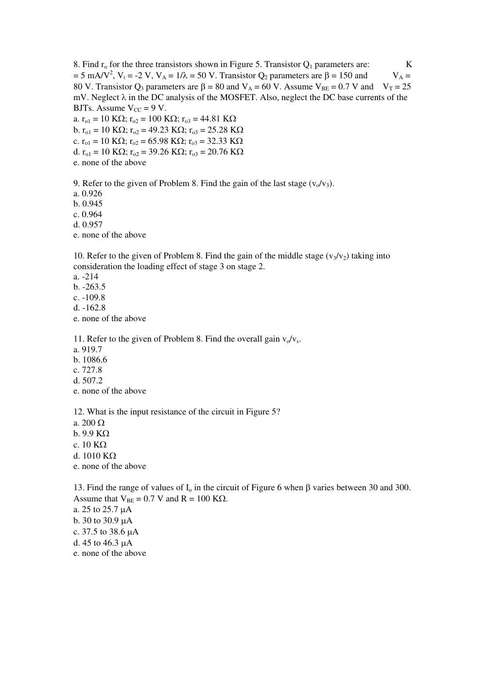
8. Find ro for the three transistors shown in Figure 5. Transistor Q1 parameters are: K
= 5 mA/V2, Vt = -2 V, VA = 1/λ = 50 V. Transistor Q2 parameters are β = 150 and VA =
80 V. Transistor Q3 parameters are β = 80 and VA = 60 V. Assume VBE = 0.7 V and VT = 25
mV. Neglect λ in the DC analysis of the MOSFET. Also, neglect the DC base currents of the
BJTs. Assume VCC = 9 V.
a. ro1 = 10 KΩ; ro2 = 100 KΩ; ro3 = 44.81 KΩ
b. ro1 = 10 KΩ; ro2 = 49.23 KΩ; ro3 = 25.28 KΩ
c. ro1 = 10 KΩ; ro2 = 65.98 KΩ; ro3 = 32.33 KΩ
d. ro1 = 10 KΩ; ro2 = 39.26 KΩ; ro3 = 20.76 KΩ
e. none of the above
9. Refer to the given of Problem 8. Find the gain of the last stage (vo/v3).
a. 0.926
b. 0.945
c. 0.964
d. 0.957
e. none of the above
10. Refer to the given of Problem 8. Find the gain of the middle stage (v3/v2) taking into
consideration the loading effect of stage 3 on stage 2.
a. -214
b. -263.5
c. -109.8
d. -162.8
e. none of the above
11. Refer to the given of Problem 8. Find the overall gain vo/vs.
a. 919.7
b. 1086.6
c. 727.8
d. 507.2
e. none of the above
12. What is the input resistance of the circuit in Figure 5?
a. 200 Ω
b. 9.9 KΩ
c. 10 KΩ
d. 1010 KΩ
e. none of the above
13. Find the range of values of Io in the circuit of Figure 6 when β varies between 30 and 300.
Assume that VBE = 0.7 V and R = 100 KΩ.
a. 25 to 25.7 µA
b. 30 to 30.9 µA
c. 37.5 to 38.6 µA
d. 45 to 46.3 µA
e. none of the above
American University of Beirut
Faculty of Engineering and Architecture
Department of Electrical and Computer Engineering
EE 042 - Analog Electronics
Instructors: L. Chaar and A. Kayssi
Quiz 1
Saturday November 14, 1998
Closed Book
Programmable Calculators Are Not Allowed.
Time: 1.5 hours
VERSION A
Name:_______________________________ ID#:__________________________
! Provide your answer on the computer card only.
! Return the computer card attached to the question sheet.
! Use a pencil for marking your answers and ID number on the computer card.
! When using an eraser, make sure you erased well.
! On this sheet, write with a pen your name followed by your ID number.
! All questions are graded equally.
1.
What is the version of your question sheet? (This question is not graded.)
a) Version A
b) Version B
c) Version C
d) Version D
e) Version E
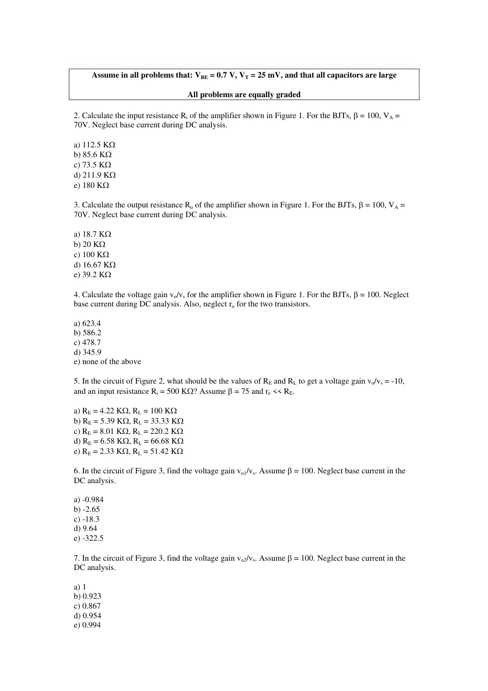
Assume in all problems that: VBE = 0.7 V, VT = 25 mV, and that all capacitors are large
All problems are equally graded
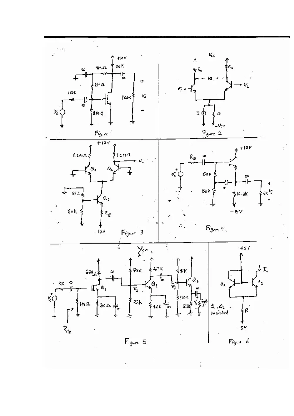
2. Calculate the input resistance Ri of the amplifier shown in Figure 1. For the BJTs, β = 100, VA =
70V. Neglect base current during DC analysis.
a) 112.5 KΩ
b) 85.6 KΩ
c) 73.5 KΩ
d) 211.9 KΩ
e) 180 KΩ
3. Calculate the output resistance Ro of the amplifier shown in Figure 1. For the BJTs, β = 100, VA =
70V. Neglect base current during DC analysis.
a) 18.7 KΩ
b) 20 KΩ
c) 100 KΩ
d) 16.67 KΩ
e) 39.2 KΩ
4. Calculate the voltage gain vo/vs for the amplifier shown in Figure 1. For the BJTs, β = 100. Neglect
base current during DC analysis. Also, neglect ro for the two transistors.
a) 623.4
b) 586.2
c) 478.7
d) 345.9
e) none of the above
5. In the circuit of Figure 2, what should be the values of RE and RL to get a voltage gain vo/vs = -10,
and an input resistance Ri = 500 KΩ? Assume β = 75 and re << RE.
a) RE = 4.22 KΩ, RL = 100 KΩ
b) RE = 5.39 KΩ, RL = 33.33 KΩ
c) RE = 8.01 KΩ, RL = 220.2 KΩ
d) RE = 6.58 KΩ, RL = 66.68 KΩ
e) RE = 2.33 KΩ, RL = 51.42 KΩ
6. In the circuit of Figure 3, find the voltage gain vo1/vs. Assume β = 100. Neglect base current in the
DC analysis.
a) -0.984
b) -2.65
c) -18.3
d) 9.64
e) -322.5
7. In the circuit of Figure 3, find the voltage gain vo2/vs. Assume β = 100. Neglect base current in the
DC analysis.
a) 1
b) 0.923
c) 0.867
d) 0.954
e) 0.994
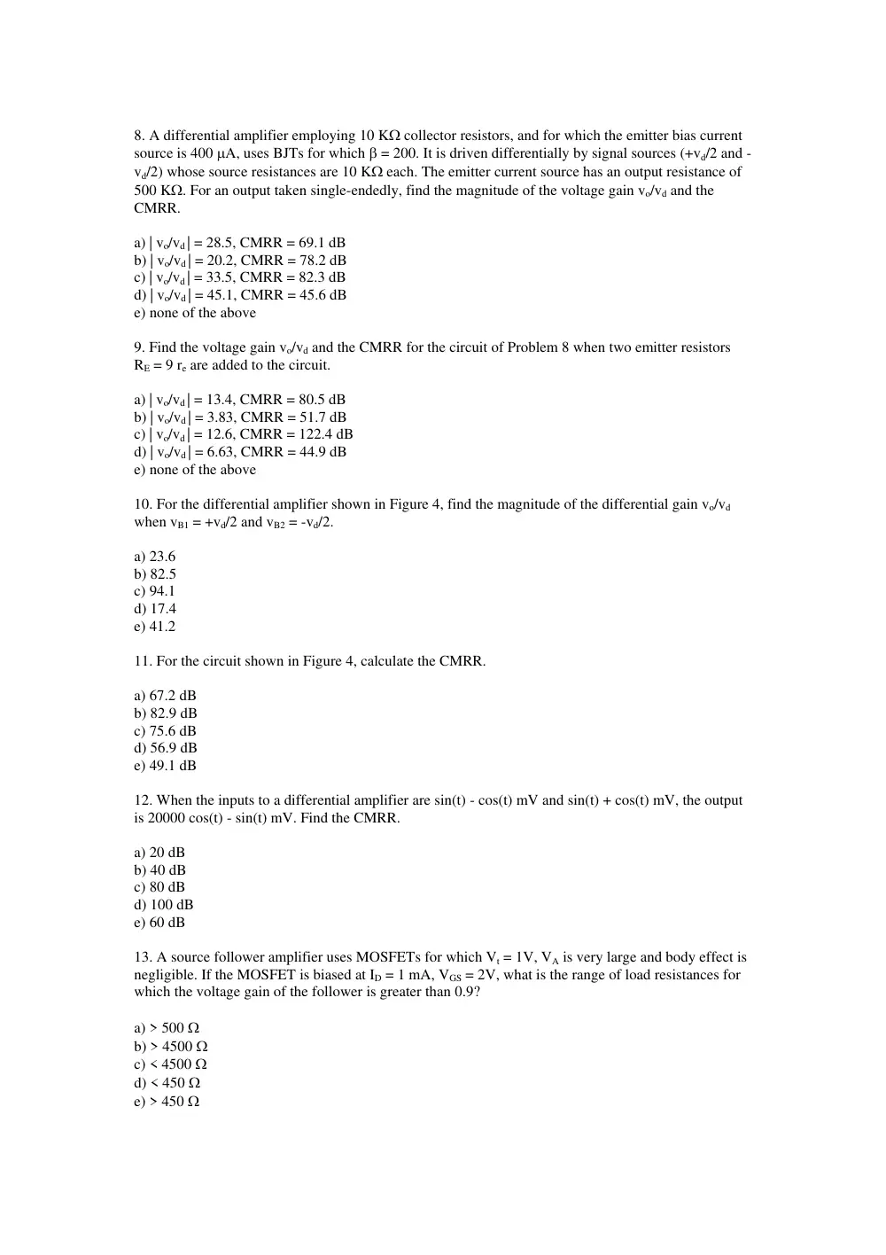
8. A differential amplifier employing 10 KΩ collector resistors, and for which the emitter bias current
source is 400 µA, uses BJTs for which β = 200. It is driven differentially by signal sources (+vd/2 and -
vd/2) whose source resistances are 10 KΩ each. The emitter current source has an output resistance of
500 KΩ. For an output taken single-endedly, find the magnitude of the voltage gain vo/vd and the
CMRR.
a) | vo/vd | = 28.5, CMRR = 69.1 dB
b) | vo/vd | = 20.2, CMRR = 78.2 dB
c) | vo/vd | = 33.5, CMRR = 82.3 dB
d) | vo/vd | = 45.1, CMRR = 45.6 dB
e) none of the above
9. Find the voltage gain vo/vd and the CMRR for the circuit of Problem 8 when two emitter resistors
RE = 9 re are added to the circuit.
a) | vo/vd | = 13.4, CMRR = 80.5 dB
b) | vo/vd | = 3.83, CMRR = 51.7 dB
c) | vo/vd | = 12.6, CMRR = 122.4 dB
d) | vo/vd | = 6.63, CMRR = 44.9 dB
e) none of the above
10. For the differential amplifier shown in Figure 4, find the magnitude of the differential gain vo/vd
when vB1 = +vd/2 and vB2 = -vd/2.
a) 23.6
b) 82.5
c) 94.1
d) 17.4
e) 41.2
11. For the circuit shown in Figure 4, calculate the CMRR.
a) 67.2 dB
b) 82.9 dB
c) 75.6 dB
d) 56.9 dB
e) 49.1 dB
12. When the inputs to a differential amplifier are sin(t) - cos(t) mV and sin(t) + cos(t) mV, the output
is 20000 cos(t) - sin(t) mV. Find the CMRR.
a) 20 dB
b) 40 dB
c) 80 dB
d) 100 dB
e) 60 dB
13. A source follower amplifier uses MOSFETs for which Vt = 1V, VA is very large and body effect is
negligible. If the MOSFET is biased at ID = 1 mA, VGS = 2V, what is the range of load resistances for
which the voltage gain of the follower is greater than 0.9?
a) > 500 Ω
b) > 4500 Ω
c) < 4500 Ω
d) < 450 Ω
e) > 450 Ω
14. The common source amplifier shown in Figure 5 uses MOSFETs for which k’(W/L) = 20 µA/V2
and VA = 100 V. How does the voltage gain vo/vs change when IREF is reduced from 100 µA to 1 µA?
a) The magnitude of the gain decreases from 316.2 to 31.6
b) The magnitude of the gain decreases from 632 to 63.2
c) The magnitude of the gain increases from 63.2 to 632
d) The magnitude of the gain increases from 31.6 to 316.2
e) There is not enough data to solve this problem.
15. Which of the following statements is true?
I. The voltage gain of an emitter-follower is much larger than 1
II. The input resistance of a common-base is very small
III. The output resistance of a common-drain is very large
IV. The current gain of common-emitter is always close to 1
a) only I is true
b) only II is true
c) only III is true
d) only IV is true
e) all are false
2K
180K
300K
300K
180K
20K
2K
18K
20K
20K
100K
Vcc = +15V
vS
+
Figure 1
RE
100 Ohm
RL
vS
vo
+
-
vo
+
-
Figure 2
Ri
Ri
1K
+
-5V
1K
+5V
vS
10K
20K
20K
vo2
+
-
vo1
+
-
Figure 3
10K
10K
+15V
+15V
82K
-15V
vB1
vB2
v0
Figure 4
IREF
vs
vo
Figure 5
+
Ro
ELEG 042 Quiz 1 – Fall 2000-2001 – Version A - Page 1 of 4
American University of Beirut
Faculty of Engineering and Architecture
Department of Electrical and Computer Engineering
ELEG 042 - Analog Electronics
Instructors: A. Kayssi and Z. Othman
Quiz 1
Thursday November 23, 2000
Closed Book
Programmable Calculators Are Not Allowed.
Time: 1.5 hours
VERSION A
Name:_______________________________ ID#:__________________________
► Provide your answer on the computer card only.
► Return the computer card attached to the question sheet.
► Use a pencil for marking your answers and ID number on the computer card.
► When using an eraser, make sure you erased well.
► On this sheet, write with a pen your name followed by your ID number.
► All questions are equally graded.
► Only the computer card will be considered in grading.
PENALTY is FOUR to ONE
1.
What is the version of your question sheet? (This question is not graded.)
a) Version A
b) Version B
c) Version C
d) Version D
e) Version E
ELEG 042 Quiz 1 – Fall 2000-2001 – Version A - Page 2 of 4
Assume in all problems that:
|VBE| = 0.7 V
VT = 25 mV
β = 100 unless otherwise specified
Capacitors are very large
Early effect is negligible unless otherwise specified
In the circuit of Figure 1, RB = 300K.
2. Find the voltage gain vo/vi.
a) –0.81
b) –0.97
c) –1.59
d) –2.34
e) –1.21
3. Find the input resistance Ri in KΩ.
a) 380.5
b) 175.8
c) 292.7
d) 339.6
e) 238.7
4. Find the current gain io/ii.
a) –41.2
b) –31.0
c) –35.4
d) –38.1
e) –33.0
In the circuit of Figure 2, assume RE = 0.5K.
5. Find the voltage gain vo/vi.
a) 0.900
b) 0.928
c) 0.952
d) 0.825
e) 0.943
6. Find Rib2 at the base of Q2 (in KΩ.)
a) 203.2
b) 253.9
c) 152.4
d) 101.6
e) 50.8
7. Find Rib1 at the base of Q1 (in MΩ.)
a) 16.39
b) 11.36
c) 21.74
d) 27.03
e) 6.17
8. Find the current gain io/ii.
a) 396.6
b) 220.1
c) 152.3
d) 94.3
e) 116.5
In the circuit of Figure 3, assume VCC = 12V.
9. Find the voltage gain vo/vi.
a) 95.2
b) 75.2
c) 35.3
d) 55.2
e) 115.2
10. Find the input resistance vi/ii in Ohms.
a) 8.5
b) 27.3
c) 13.0
d) 17.6
e) 10.3
In the circuit of Figure 4, assume I = 2.5mA.
11. Find the differential voltage gain (vc1 – vc2)/vd, when vB1 = +vd/2 and vB2 = -vd/2.
a) –9.9
b) –11.3
c) –12.4
d) –13.2
e) –11.9
ELEG 042 Quiz 1 – Fall 2000-2001 – Version A - Page 3 of 4
12. Find the differential input resistance Rid in KΩ.
a) 26.5
b) 30.3
c) 22.7
d) 25.3
e) 24.2
13. Find the input bias current in microAmps when β1=80 and β2=120.
a) 12.88
b) 5.15
c) 10.31
d) 20.61
e) 8.24
14. Find the input offset current in microAmps when β1=80 and β2=120.
a) 4.08
b) 8.16
c) 5.10
d) 2.04
e) 3.26
15. A differential amplifier has a CMRR of 70 dB. The output voltage is 100 mV when
the inputs are v1 = 21.5 mV and v2 = 20 mV. Find the differential gain of this amplifier.
a) 66.4
b) 53.5
c) 58.6
d) 46.4
e) 63.9
In the circuit of Figure 5, the MOSFETs have Vt = 2.2V and ½ k’n(W/L) = 1 mA/V2.
Neglect body effect and channel length modulation.
16. Find ID in mA.
a) 0.090
b) 0.0563
c) 0.116
d) 0.0730
e) 0.160
17. Find gm for the MOSFETs in mA/V.
a) 0.600
b) 0.540
c) 0.474
d) 0.800
e) 0.681
18. Find vo1/vs.
a) –5.12
b) –5.68
c) –7.58
d) –4.49
e) –6.45
19. Find vo2/vs.
a) 18.4
b) 29.3
c) 22.7
d) 40.4
e) 14.2
20. Find ro in KΩ for the MOSFETs given that channel length modulation for AC signals is not
negligible and is modeled by λ = 0.1 V-1.
a) 62.5
b) 177.7
c) 137.0
d) 111.1
e) 86.2
21. Find Ro in KΩ, given that channel length modulation for AC signals is not negligible and is
modeled by λ = 0.1 V-1.
a) 16.9
b) 17.5
c) 16.2
d) 15.2
e) 18.0
ELEG 042 Quiz 1 – Fall 2000-2001 – Version A - Page 4 of 4
1000K
vi
vo
0.1K
10K
10K
+10V
vi
vo
500K
500K
10K
RE
+12V
vi
vo
Vcc
1K
1K
+10V
1K
2K
0.1K
0.1K
I
Q1
Q2
RB
Ri
io
ii
Q2
Q1
Rib2
ii
Rib1
io
500K
io
ii
vB1
vB2
vC1
vC2
+12V
300K
300K
100K
20K
20K
10K
10K
50K
10K
vo2
vs
+
100K
vo1
ID
Ro
Figure 1
Figure 2
Figure 3
Figure 4
Figure 5
ELEG 042 Quiz 1 – Fall 2000-2001 – All Versions - Page 4 of 4
ELEG 042 Quiz 1 – Fall 2001-2002 – Page 1 of 4
American University of Beirut
Faculty of Engineering and Architecture
Department of Electrical and Computer Engineering
ELEG 042 - Analog Electronics
Instructors: A. Kayssi and Z. Othman
Quiz 1
November 2001
Closed Book
Programmable Calculators Are Not Allowed.
Time: 1.5 hours
Name:_______________________________ ID#:__________________________
► Provide your answer on the computer card only.
► Return the computer card attached to the question sheet.
► Use a pencil for marking your answers and ID number on the computer card.
► When using an eraser, make sure you erased well.
► On this sheet, write with a pen your name followed by your ID number.
► All questions are equally graded.
► Only the computer card will be considered in grading.
PENALTY is FOUR to ONE
Penalty is calculated as follows:
One to three wrong answers result in no penalty; four to seven wrong answers result
in canceling one correct answer; eight to eleven wrong answers result in canceling
two correct answers; and so on.
ELEG 042 Quiz 1 – Fall 2001-2002 – Page 2 of 4
Assume in all problems that:
|VBE| = 0.7 V
VT = 25 mV
β = 100 unless otherwise specified
Capacitors are very large
Early effect and body effect are negligible unless otherwise specified
In the circuit of Figure 1, I2 = I3 = 0.24 mA.
1. Find the collector current of transistor Q2 in mA.
a) 1.21
b) 0.667
c) 0.242
d) 0.828
e) 0.354
2. Find the collector current of transistor Q1 in µA.
a) 2.4
b) 12
c) 6.6
d) 8.2
e) 3.5
3. Find the input resistance at the base of Q2 (Ri2) in KΩ.
a) 3.75
b) 2.06
c) 10.3
d) 3.02
e) 7.07
4. Find the input resistance at the base of Q1 (Ri) in MΩ.
a) 0.758
b) 0.610
c) 0.417
d) 1.43
e) 2.08
5. Find the voltage gain vc2/vb2 (vc2 and vb2 are the small-signal collector and base voltages of
transistor Q2, respectively.)
a) –138.7
b) –475.4
c) –261.5
d) –95.1
e) –324.9
6. Find the voltage gain vo/vi
a) –68.4
b) –236.7
c) –46.6
d) –161.5
e) –129.8
7. Find the output resistance Ro in Ohms.
a) 116.8
b) 125.9
c) 164.2
d) 194.3
e) 132.9
In the circuit of Figure 2, assume the DC value of the output voltage to be VO = -2 V.
The MOSFET parameters are Vtn = 0.8 V, ½ k’n(W/L)n = 0.5 mA/V2, λn = 0.01 V-1, and
Vtp = - 0.8 V, ½ k’p(W/L)p = 0.2 mA/V2, λp = - 0.01 V-1.
8. Find VGS for transistor Q2 in Volts.
a) 1.86
b) 1.66
c) 2.03
d) 1.41
e) 2.18
9. Find ID of Q1 in mA.
a) 0.139
b) 0.205
c) 0.105
d) 0.0687
e) 0.172
10. Find the voltage gain vo/vg2 (vg2 is the small-signal voltage at the gate of Q2.)
a) 0.862
b) 0.846
c) 0.820
d) 0.873
e) 0.766
11. Find the voltage gain vo/vi
a) –9.65
b) –8.26
c) –6.37
d) –10.8
e) –11.7
In the circuit of Figure 3, assume I = 250 µA and RB = 30 K.
12. Find the value of RE (in KΩ) to get the specified I when v1 = v2 = 0.
a) 37.1
b) 30.9
c) 92.9
d) 61.9
e) 46.4
13. Find Ad = vo2 / vd when v1 = +vd/2 and v2 = – vd/2
a) 49.8
b) 31.1
c) 39.3
d) 45.2
e) 53.4
ELEG 042 Quiz 1 – Fall 2001-2002 – Page 3 of 4
14. Find Acm = vo2/vcm when v1 = v2 = vcm
a) –0.664
b) –0.531
c) –0.266
d) –0.796
e) –0.398
15. Find the CMRR in dB, corresponding to the values of the gains calculated in the previous
two questions.
a) 41.4
b) 37.5
c) 36.5
d) 38.6
e) 39.9
16. Find the differential input resistance vd / ib1 in KΩ, when v1 = +vd/2 and v2 = – vd/2.
a) 127.3
b) 100.4
c) 161
d) 110.5
e) 93.7
17. Find the common-mode input resistance vcm/(2ib1) in MΩ, when v1 = v2 = vcm
a) 3.14
b) 9.42
c) 4.71
d) 6.28
e) 3.77
18. Find the input bias current in µA.
a) 0.743
b) 1.238
c) 0.495
d) 0.990
e) 1.485
19. Find the input offset current (in nA) when β is matched to within +/- 1.5%.
a) 22.3
b) 37.1
c) 29.7
d) 14.9
e) 44.6
A differential amplifier has a differential voltage gain of 350 and a CMRR of 85 dB. A
differential input signal of vd = 2 sin(ωt) mV is applied, along with a common-mode voltage of
vcm = 2 sin(ωt) V. Assume that the common-mode gain is positive.
20. Determine the amplitude of the ideal output voltage in Volts.
a) 0.7
b) 0.6
c) 0.3
d) 0.5
e) 0.4
21. Determine the amplitude of the actual output voltage in Volts.
a) 0.528
b) 0.638
c) 0.422
d) 0.739
e) 0.317
In the circuit of Figure 4, assume Vcc = 7 V.
22. Find the collector current of the BJT in mA.
a) 1.71
b) 1.49
c) 1.26
d) 0.811
e) 1.04
23. Find the value of re for the BJT in Ohms.
a) 23.9
b) 30.5
c) 16.7
d) 19.6
e) 14.5
24. Find the input resistance Ri in KΩ.
a) 148.4
b) 142.4
c) 145.8
d) 137.9
e) 131.4
25. Find minimum value of the total output voltage in Volts when vs = sin(ωt) Volt.
a) 2.076
b) 1.624
c) 2.529
d) 0.725
e) 1.174
ELEG 042 Quiz 1 – Fall 2001-2002 – Page 4 of 4
Figure 3
Figure 2
vi
vo
10K
Vcc
Q2
Q1
Ri
Figure 1
5K
+
-
Q3
Ro
I2
I3
Ri2
vi
vo
35K
5K
-5V
+5V
Q1
Q2
+10V
50K
50K
Q1
Q2
v1
v2
vO1
vO2
-10V
RE
RB
RB
+
+
I
Figure 4
vo
Vcc
10K
10K
20K
2K
Ri
20K
Vcc
+
vs
American University of Beirut
Department of Electrical and Computer Engineering
EECE 311 – Electronics II
Instructor: Ayman Kayssi
Final Exam
January 21, 2006
Open Book
Time: 180 minutes
Name:
ID Number:
Problem 1 [10 points]
a) Refer to the circuit shown in Figure 1. What should be the value of R in order to
have class AB operation? Assume |VBE(on)| = 0.65 V and neglect base current. Note
that the bias circuit of Q1 has negligible effect and is not shown.
b) The average DC current drawn from each of the two power supplies is 20 mA.
What is the efficiency of the amplifier if the peak-to-peak output voltage is 10 V?
vs
+
R
0.2 mA
100 Ω
-15 V
+15 V
10K
C
Q1
Figure 1
Problem 2 [20 points]
a) For the amplifier circuit shown in Figure 2, assume VD = 0.7 V for a conducting
diode, VBE = 0.7 V, and VCE(edge of sat) = 0.3 V. The BJTs are identical and have
negligible base current. The FETs are identical with k’n (W/L) = 2.5 mA/V2 and Vt =
1 V. Find VOUT when V1 = V2 = 0.
b) Find the total circuit power dissipation when V1 = V2 = 0.
c) Find the input common-mode range.
-10V
+10V
-10V
+10V
-10V
10K
Vout
5K
14.3K
2.6K
-10V
5K
14.3K
+10V
+10V
10K
10K
+10V
10K
10K
+10V
15.3K
-6V
-10V
4K
V
V
1
2
V s
Figure 2
Problem 3 [20 points]
Consider the amplifier shown in Figure 3. For the MOSFET, gm = 10 mA/V, and Cgs =
Cgd = 0.1 pF. For the BJT, β = 100, gm = 50 mA/V, Cπ = 1 pF and Cμ = 0.5 pF.
a) Find the midband gain vo/vs.
b) Find the upper 3-dB frequency using Miller’s theorem and the open circuit time
constants method.
Figure 3
Problem 4 [20 points]
Design a low-pass Butterworth filter to meet the following specs:
Amax = 2.5 dB
Amin = 20 dB
fP = 15 KHz
fS = 25 KHz
Show the op-amp implementation of the filter. Minimize the number of op-amps in
your implementation, and use 1 nF capacitors whenever possible.
Q 1
10K
V S
+
10K
V o
Vbias
Vcc
Q 2
Problem 5 [15 points]
5V
- 5V
Q3
Q4
Q2
Q1
Q5
Q6
Q10
Q7
Q8
Q9
IREF
v2
v1
Q11
Figure 4
Consider the circuit shown in Figure 4.
a) What is the inverting input for this op-amp? Explain.
b) Find the output resistance of the op-amp. Assume that k’n = 25 μA/V2, k’p = 10
μA/V2, Vtn = 0.75 V, Vtp = -0.75 V, and IREF = 100 μA. The sizes of the MOSFETs are
as follows: (W/L)1 = (W/L)2 = (W/L)9 = (W/L)10 = 20
(W/L)3 = (W/L)4 = 50
(W/L)6 = (W/L)8 = 10
(W/L)5 = 100
(W/L)7 = 25
(W/L)11 = 5
Problem 6 [15 points]
The op-amp shown in Figure 5 is modeled by an infinite input resistance, an open-
loop open-circuit differential voltage gain function of 107/(s+50), and an output
resistance of 500 Ω. What is the maximum load capacitance CL that can be connected
at the output of a voltage follower configuration (as shown in the figure), if the phase
margin of the amplifier is 60 degrees?
Vo
Vi
+
-
+
CL
Figure 5
American University of Beirut
Department of Electrical and Computer Engineering
EECE 311 – Electronics II
Fall 2005 – 2006 (Section 2)
Quiz 1 – Solution
Problem 1:
v i
Q 1
V I
I
v O
a) I = ½ k’n (W/L) (VGS – Vtn)2
=> 40 u = 0.5 (0.2m)(5)(VI – 0.5)2
=> VI = 0.5 + sqrt(40u/0.5m) = 0.783 V
b) vO = vDS => vOmin = vDSmin = vGS – Vtn
Assuming vGS = VGS (DC value) => vOmin = 0.783 – 0.5 = 0.283 V
c) gm = ID/(VOV/2) = 40u/(0.283/2) = 0.283 mA/V
ro = VA/ID = (1/0.1) / 40u = 250 K
gain = vo/vi = –gm(ro // Ro of current source) = –0.283(100//250) = –20.2 V/V
Q3
IREF
VSG
+
-
Q2
d) ID(Q2) = ½ k’p (W/L) (VOV2)2
This current is equal to 40u
=> 40u = 0.5(0.08m)(W/L)(0.2)2 => (W/L) = 25 for Q2
(W/L) = 25 for Q3, since Q2 and Q3 are matched.
e) VSG = |Vtp| + |VOV2| = 0.54 + 0.2 = 0.74 V
f) Output resistance is ro2 = VAP / ID2 = (1/0.12) / 40u = 208.33 K
g) For Q2: |VDS| ≥ |VGS| – |Vtp| => VDD – VO ≥ 0.2 V => VOmax = VDD – 0.2 V
Problem 2:
In this problem, there is an implicit assumption that the signal source (not shown) has
a large source resistance, and that the source does not affect the DC bias.
I
vi
+
-
vo
RB
300K
RL
10K
CL
20pF
a) DC analysis: current in 300K resistor = IB
KCL at collector: 0.5 mA = IB + IC + VO/10K
But VO = 300K×IB + VBE = 300K×IB + 0.7 V
=> 0.5 mA = IB + β IB + (300K×IB + 0.7 V)/10K
=> 0.5 mA – 0.07 mA = 91 IB => IB = 4.725 uA
IC = 60 IB = 0.2835 mA
VO = 300K×4.725 uA + 0.7 V = 2.118 V
b) The Miller constant is the gain from base to collector without RB, and is given by
–gm R’L with R’L = ro (BJT) // Ro (current source) // RL
ro (BJT) = VA/IC = 80/0.2835m = 282.2 K
R’L = 282.2 K // 100 K // 10K = 8.807 K
gm = IC/VT = 0.2835m/25m = 11.34 mA/V
Miller’s K = –gm R’L = –11.34×8.807 = –99.87
Equivalent resistance from base to ground due to RB: R1 = RB/(1 – K) =
300K/(1+99.87) = 2.974 K
The input resistance is Rin = rπ // R1
rπ = VT/IB = 25m/4.725u = 5.291 K
Rin = 5.291 // 2.974 = 1.904 K
c) The resistance seen by Cπ is Rin (we can use the approximation from part (b)) =
1.904 K. The more accurate estimate is obtained as follows:
iRB = (vi – vo)/RB = (1 – gain)vi/RB => vi/iRB = RB/(1 – gain) = 300K/(1 + 97) = 3.061
K [note: the value of the voltage gain is found in part (d)]
Resistance seen by Cπ is equal to: rπ // (vi/iRB) = 5.291 K // 3.061 K = 1.939 K
rpi
RB
gmvi
R’L
vi
vo
Resistance
seen by Cpi
Resistance
seen by Cmu
Resistance
seen by CL
The resistance seen by CL is equal to:
R’L // (resistance due to controlled source) // (RB + rπ):
vπ = vi = vx rπ/(rπ+RB) = vx×5.291/(5.291+300) = vx/57.7
The controlled current source is therefore equivalent to a resistance equal to 57.7/gm =
5.088 K
The resistance seen by CL is therefore: 8.807 // 5.088 // 305.29 = 3.191 K
The resistance seen by Cμ is equal to: RB // (R’L + rπ + gm×rπ×R’L) = 300 K // (8.807
K + 5.291 K + 11.34×8.807×5.291 K) = 193.2 K.
τH = 1.939 K×1 pF + 3.191 K×20 pF + 193.2 K×1 pF = 258.96 nsec
fH = 1/(2π τH) = 614.6 KHz
d) The low-frequency voltage gain is determined without using Miller’s theorem. The
current in RB is (vi – vo)/RB. This current is equal to gm vi + vo/R’L. Therefore:
(1/RB – gm) vi = vo(1/R’L + 1/RB) => The voltage gain is
vo/vi = (1/RB – gm)/ (1/R’L + 1/RB) = (1 – gm RB)/(RB/R’L + 1)
= (1 – 11.34×300)/(300/8.807+1) = –97 V/V or 39.74 dB
e) Asymptotic Bode Plot
Gain in dB
39.74
614.6 KHz
f (log scale)
-20 dB/dec
Problem 3
IREF
R1
10K
R2
10K
IO
2V
VO
a) IREF = (2 – VGS1)/10K = ½ k’n (W/L) (VGS1 – Vtn)2 = (0.5)(0.2m)(10)(VGS1 – 0.4)2.
Solving the quadratic equation we get: VGS = 0.753 V (the other root is negative).
IREF is therefore (2 – 0.753)/10K = 0.1247 mA
b) VGS2 = VGS1 – IO×R2 and
IO = ½ k’n (W/L) (VGS2 – Vtn)2 = ½ k’n (W/L)(VGS1 – IO×R2 – Vtn)2
Therefore IO = (0.5)(0.2m)(10)(0.753 – IO×10K – 0.4)2
=> IO = 20.86 uA
The value of VGS2 is 0.753 – 20.86u×10K = 0.5444 V
c) The minimum output voltage corresponds to VDS2 = VGS2 – Vtn => VO – IOR2 =
VGS2 – Vtn => VOmin = 20.86u×10K + 0.5444 – 0.4 = 0.353 V
d) The output resistance is given by ro2 + R2 + gm2 ro2 R2
ro2 = VA/IO = (1/0.08)/20.86u = 599.23 K
gm2 = IO/(VOV/2) = 20.86u/((0.5444-0.4)/2) = 0.289 mA/V
RO is therefore equal to: 10K + 599.23K + 599.23K×0.289m×10K = 2340.5 K
Problem 4
In this problem, there is an implicit assumption that the signal source (not shown) has
a large source resistance.
vo
vi
vo
vi
VDC
a) Using Miller’s theorem, the time constant at the input of the circuit is given by
τH = rπ (Cπ + Cμ (1 + gm ro)) since the only “load” is the output resistance of the BJT
itself.
τH = rπ (Cπ + Cμ (1 + gm ro)) = rπCπ + rπCμ + rπCμgm ro = rπCπ + rπCμ + βroCμ
The third term is much larger than the first two, and therefore τH is approximately
βroCμ.
fH = 1/(2π τH) = 1/(2π βroCμ)
b) The current source output resistance is approximately ro. The output resistance of
the amplifier becomes Ro ≈ ro//ro = ro/2. The open-circuit voltage gain becomes –gm
ro/2 = –A0/2. The 3-dB frequency becomes 1/(2π τH) = 1/(2π β(ro/2)Cμ) = 2 fH
c) The current source output resistance is approximately βro. The output resistance of
the amplifier becomes Ro ≈ βro//ro ≈ ro. The open-circuit voltage gain becomes –gmro
= –A0. The 3-dB frequency becomes 1/(2π τH) = 1/(2π βroCμ) = fH
d) For an unloaded cascode amplifier, the output resistance of the unloaded amplifier
is given by βro. The output resistance of the amplifier becomes Ro ≈ βro//ro ≈ ro. The
open-circuit voltage gain becomes (see Fig. 6.41 in textbook) –βA0 ro/(ro+βro) ≈ –A0.
The 3-dB frequency becomes 1/(2π τH) ≈ 1/(2π roCμ) = βfH (see Fig. 6.42 in
textbook)
e) The output resistance of the amplifier becomes Ro ≈ βro//βro = βro/2. The open-
circuit voltage gain becomes –βA0 βro/(βro+βro) = –βA0/2. The 3-dB frequency
becomes 1/(2π τH) ≈ 1/(2π (βro/2)Cμ) = 2fH
Problem 5
R1
R2
R3
vi2
vo
R4
vi1
For the difference amplifier, the output voltage is given by:
2
4
2
1
3
4
1
1
2
(1
)
R
R
R
o
i
i
R
R
R
R
v
v
v
−
+
=
+
+
=>
1
2
4.7
4.674
o
i
i
v
v
v
= −
+
= Av1 vi1 + Av2 vi2 = Ad (vi1 – vi2) + Acm (vi1+vi2)/2
=> Ad = (Av1 – Av2)/2 = –4.687 V/V
and Acm = Av1 + Av2 = –0.026 V/V
=> CMRR = 20 log|4.687/0.026| = 45.12 dB
EECE 311 Quiz 2 Page 1 of 7
American University of Beirut
Departmen