
EECE 412 Project, Spring 2008
American University of Beirut · Digital Integrated Circuits · 2 pages
More EECE 412 files
Show the text of this project
Prof. M. Mansour
American University of Beirut
Department of Electrical and Computer Engineering
EECE 412/612 – Digital Integrated Circuits
Fall 2008
Project
(Due on January 23, 2009)
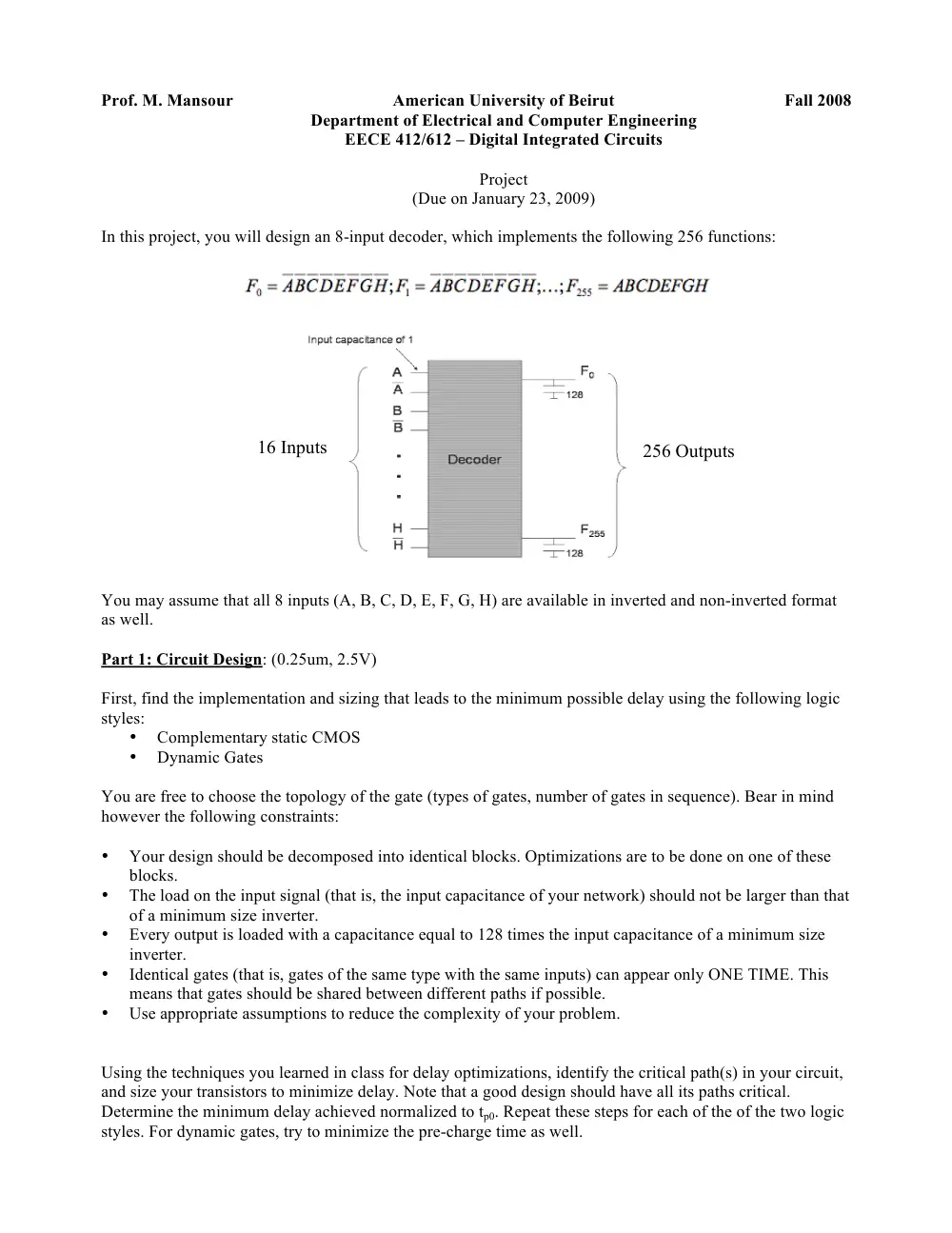
In this project, you will design an 8-input decoder, which implements the following 256 functions:
You may assume that all 8 inputs (A, B, C, D, E, F, G, H) are available in inverted and non-inverted format
as well.
Part 1: Circuit Design: (0.25um, 2.5V)
First, find the implementation and sizing that leads to the minimum possible delay using the following logic
styles:
•
Complementary static CMOS
•
Dynamic Gates
You are free to choose the topology of the gate (types of gates, number of gates in sequence). Bear in mind
however the following constraints:
•
Your design should be decomposed into identical blocks. Optimizations are to be done on one of these
blocks.
•
The load on the input signal (that is, the input capacitance of your network) should not be larger than that
of a minimum size inverter.
•
Every output is loaded with a capacitance equal to 128 times the input capacitance of a minimum size
inverter.
•
Identical gates (that is, gates of the same type with the same inputs) can appear only ONE TIME. This
means that gates should be shared between different paths if possible.
•
Use appropriate assumptions to reduce the complexity of your problem.
Using the techniques you learned in class for delay optimizations, identify the critical path(s) in your circuit,
and size your transistors to minimize delay. Note that a good design should have all its paths critical.
Determine the minimum delay achieved normalized to tp0. Repeat these steps for each of the of the two logic
styles. For dynamic gates, try to minimize the pre-charge time as well.
16 Inputs
256 Outputs
Deliverables:
•
Two designs using the two logic styles neatly drawn. All transistors must be appropriately sized.
Justify the sizing of your transistors.
•
A table comparing the delays of your circuits.
Part 2: HSPICE Verification
Using HSPICE, verify the delay computations you determined in the previous part, and report the percentage
error. For each case, determine the highest power consumption of your circuit through simulation assuming
only one input is allowed to switch. Which of the logic styles results is best in terms of power consumption?
Deliverables:
•
Two HSPICE netlists that can be used to reproduce your results.
•
A table comparing the delays of your circuits achieved using HSPICE as well as the delays
computed above. Also include the measured power in each case.