
EECE 290 Final, Spring 2015
American University of Beirut · Analog Signal Processing · 8 pages · Prof. Nassir Sabah


More EECE 290 files
- Final Sabah · Spring 2017Final examView
- Exam 1 Clean Copy · Spring 2019ExamView
- Lecture Slides Problem Solving Complex Power 2 · Spring 2019LabView
- Lecture Slides Problem Solving Convolution · Spring 2019LabView
- Exam 2 Clean Copy · Spring 2019ExamView
- Exam 1 with Solutions · Spring 2019Exam · with solutionView
- Lecture Slides Problem Solving Butterworth · Spring 2019LabView
- Lecture Slides Problem Solving Active Filters · Spring 2019LabView
Show the text of this final exam
t, s
10
2
4
vSRC1, V
t, s
-A
2
4
vSRC2, V
+
–
vO
1 k
–
+
2 k
–
+
0.1 F
vSRC1
vSRC2
–
+
+
–
10
–
+
1 F
vSRC
–
+
vO
t, s
f(t)
1
1
2
-1
-2
3
4
2
1
3
2
4
t, s
1
-1
-2
5
6
0
EECE 290
Final Exam, May 13, 2015
3%
A. Determine vO(t), assuming vSRC = 0.1u(t) V.
Solution: vO(t) = -CRdvSRC/dt = -100.1(t) = -(t) V
3%
B. Determine the rms value of the periodic function
whose first period is shown.
Solution: The area under the square of the first half cycle
Is 1 + 4 + 1 = 6. The mean is 2 and the rms value is .
3%
C. Convolve tu(t) with tu(t).
Solution: .
3%
D. Derive the Fourier transform of f(t).
Solution: f(t) = u(-t) + u(t – 2); F(j) =
+
.
3%
1.
vSRC1(t) and
vSRC2(t) are the
periodic
functions
shown.
Determine
so that vO(t) is
periodic, assuming
A = 16 V.
A. 1 s
B. 0.2 s
C. 0.5 s
D. 1.25 s
E. 2.5 s
Solution: For vO(t) to be periodic, the average current through the capacitor must be zero.
p1/8
C1
C2
C3
C4
t = 0
–
+
2 V
–
+
4 V
+
–
v3
+
–
v4
2 F
4 F
1 F
2 F
ffw(t)
t, s
1
1
2
-1
-2
1
2
-1
-2
1
0.6
(a)
(b)
t, s
1 mH
C
–
+
VSRC
This requires that , where VSRC1 and VSRC2 are the respective dc components, that is, VSRC1 =
5 V and VSRC2 = -A/2. This gives: , or = 20/A s.
Version 1: A = 16; = 20/16 = 1.25 s
Version 2: A = 20; = 20/20 = 1 s
Version 3: A = 40; = 20/40 = 0.5 s
Version 4: A = 80; = 20/80 = 0.25 s
Version 5: A = 100; = 20/100 = 0.2 s.
3%
2.
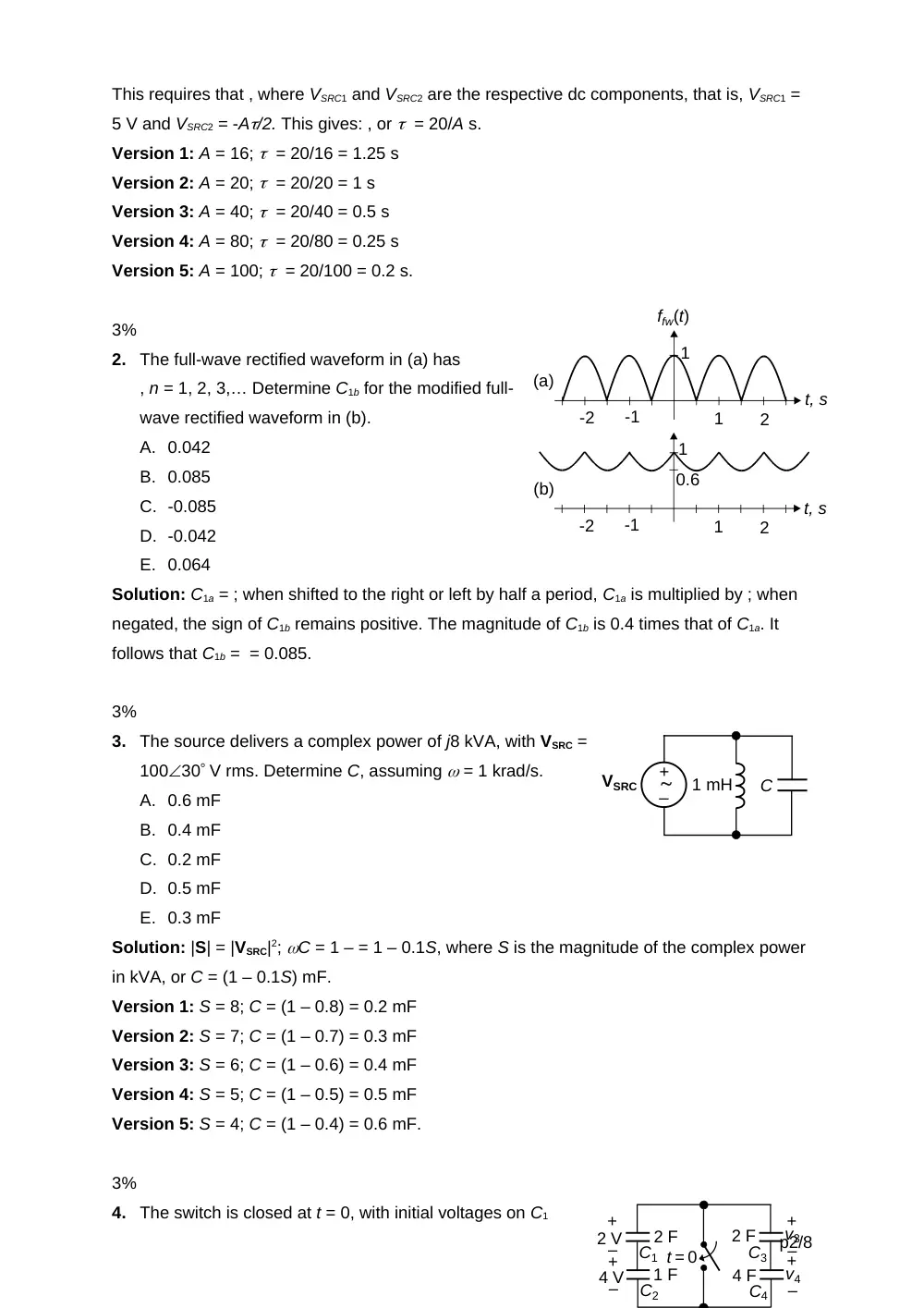
The full-wave rectified waveform in (a) has
, n = 1, 2, 3,… Determine C1b for the modified full-
wave rectified waveform in (b).
A. 0.042
B. 0.085
C. -0.085
D. -0.042
E. 0.064
Solution: C1a = ; when shifted to the right or left by half a period, C1a is multiplied by ; when
negated, the sign of C1b remains positive. The magnitude of C1b is 0.4 times that of C1a. It
follows that C1b = = 0.085.
3%
3.
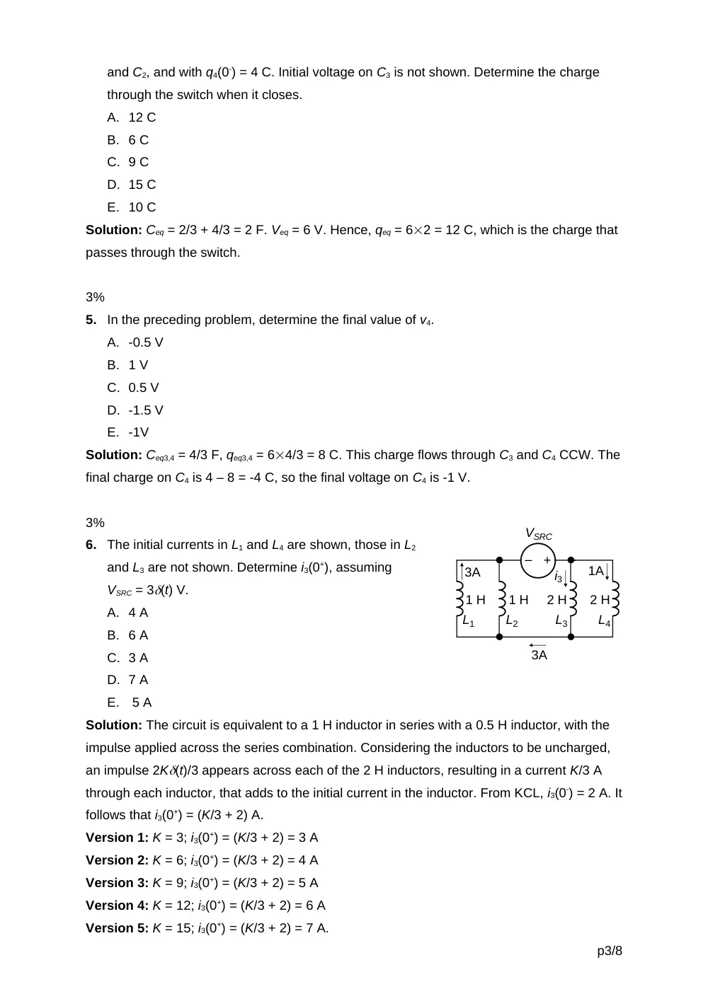
The source delivers a complex power of j8 kVA, with VSRC =
10030 V rms. Determine C, assuming = 1 krad/s.
A. 0.6 mF
B. 0.4 mF
C. 0.2 mF
D. 0.5 mF
E. 0.3 mF
Solution: |S| = |VSRC|2; C = 1 – = 1 – 0.1S, where S is the magnitude of the complex power
in kVA, or C = (1 – 0.1S) mF.
Version 1: S = 8; C = (1 – 0.8) = 0.2 mF
Version 2: S = 7; C = (1 – 0.7) = 0.3 mF
Version 3: S = 6; C = (1 – 0.6) = 0.4 mF
Version 4: S = 5; C = (1 – 0.5) = 0.5 mF
Version 5: S = 4; C = (1 – 0.4) = 0.6 mF.
3%
4.
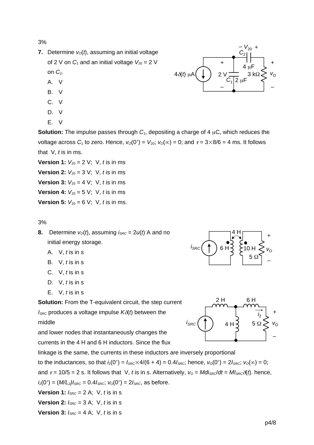
The switch is closed at t = 0, with initial voltages on C1
p2/8
–
+
2 H
2 H
1 H
1 H
L1
L2
L3
L4
1A
3A
3A
i3
VSRC
and C2, and with q4(0-) = 4 C. Initial voltage on C3 is not shown. Determine the charge
through the switch when it closes.
A. 12 C
B. 6 C
C. 9 C
D. 15 C
E. 10 C
Solution: Ceq = 2/3 + 4/3 = 2 F. Veq = 6 V. Hence, qeq = 62 = 12 C, which is the charge that
passes through the switch.
3%
5.
In the preceding problem, determine the final value of v4.
A. -0.5 V
B. 1 V
C. 0.5 V
D. -1.5 V
E. -1V
Solution: Ceq3,4 = 4/3 F, qeq3,4 = 64/3 = 8 C. This charge flows through C3 and C4 CCW. The
final charge on C4 is 4 – 8 = -4 C, so the final voltage on C4 is -1 V.
3%
6.
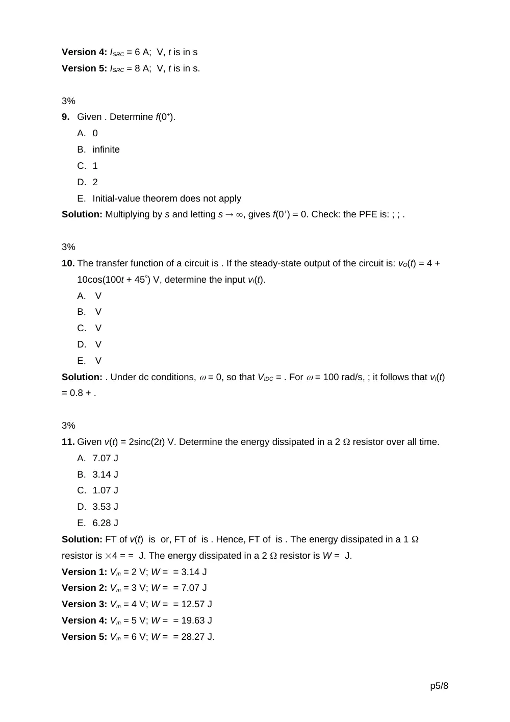
The initial currents in L1 and L4 are shown, those in L2
and L3 are not shown. Determine i3(0+), assuming
VSRC = 3(t) V.
A. 4 A
B. 6 A
C. 3 A
D. 7 A
E. 5 A
Solution: The circuit is equivalent to a 1 H inductor in series with a 0.5 H inductor, with the
impulse applied across the series combination. Considering the inductors to be uncharged,
an impulse 2K(t)/3 appears across each of the 2 H inductors, resulting in a current K/3 A
through each inductor, that adds to the initial current in the inductor. From KCL, i3(0-) = 2 A. It
follows that i3(0+) = (K/3 + 2) A.
Version 1: K = 3; i3(0+) = (K/3 + 2) = 3 A
Version 2: K = 6; i3(0+) = (K/3 + 2) = 4 A
Version 3: K = 9; i3(0+) = (K/3 + 2) = 5 A
Version 4: K = 12; i3(0+) = (K/3 + 2) = 6 A
Version 5: K = 15; i3(0+) = (K/3 + 2) = 7 A.
p3/8
2 F
3 k
–
+
vO
4 F
–
+
2 V
4(t) A
+
– V20
C1
C2
5
–
+
vO
2 H
4 H
6 H
iSRC
i2
5
–
+
vO
10 H
6 H
4 H
iSRC
3%
7.
Determine vO(t), assuming an initial voltage
of 2 V on C1 and an initial voltage V20 = 2 V
on C2.
A. V
B. V
C. V
D. V
E. V
Solution: The impulse passes through C1, depositing a charge of 4 C, which reduces the
voltage across C1 to zero. Hence, vO(0+) = V20; vO() = 0; and = 38/6 = 4 ms. It follows
that V, t is in ms.
Version 1: V20 = 2 V; V, t is in ms
Version 2: V20 = 3 V; V, t is in ms
Version 3: V20 = 4 V; V, t is in ms
Version 4: V20 = 5 V; V, t is in ms
Version 5: V20 = 6 V; V, t is in ms.
3%
8.
Determine vO(t), assuming iSRC = 2u(t) A and no
initial energy storage.
A. V, t is in s
B. V, t is in s
C. V, t is in s
D. V, t is in s
E. V, t is in s
Solution: From the T-equivalent circuit, the step current
ISRC produces a voltage impulse K(t) between the
middle
and lower nodes that instantaneously changes the
currents in the 4 H and 6 H inductors. Since the flux
linkage is the same, the currents in these inductors are inversely proportional
to the inductances, so that i2(0+) = ISRC4/(6 + 4) = 0.4ISRC; hence, vO(0+) = 2ISRC; vO() = 0;
and = 10/5 = 2 s. It follows that V, t is in s. Alternatively, vO = MdiSRC/dt = MISRC(t). hence,
i2(0+) = (M/L2)ISRC = 0.4ISRC; vO(0+) = 2ISRC, as before.
Version 1: ISRC = 2 A; V, t is in s
Version 2: ISRC = 3 A; V, t is in s
Version 3: ISRC = 4 A; V, t is in s
p4/8
Version 4: ISRC = 6 A; V, t is in s
Version 5: ISRC = 8 A; V, t is in s.
3%
9.
Given . Determine f(0+).
A. 0
B. infinite
C. 1
D. 2
E. Initial-value theorem does not apply
Solution: Multiplying by s and letting s , gives f(0+) = 0. Check: the PFE is: ; ; .
3%
10. The transfer function of a circuit is . If the steady-state output of the circuit is: vO(t) = 4 +
10cos(100t + 45) V, determine the input vI(t).
A. V
B. V
C. V
D. V
E. V
Solution: . Under dc conditions, = 0, so that VIDC = . For = 100 rad/s, ; it follows that vI(t)
= 0.8 + .
3%
11. Given v(t) = 2sinc(2t) V. Determine the energy dissipated in a 2 resistor over all time.
A. 7.07 J
B. 3.14 J
C. 1.07 J
D. 3.53 J
E. 6.28 J
Solution: FT of v(t) is or, FT of is . Hence, FT of is . The energy dissipated in a 1
resistor is 4 = = J. The energy dissipated in a 2 resistor is W = J.
Version 1: Vm = 2 V; W = = 3.14 J
Version 2: Vm = 3 V; W = = 7.07 J
Version 3: Vm = 4 V; W = = 12.57 J
Version 4: Vm = 5 V; W = = 19.63 J
Version 5: Vm = 6 V; W = = 28.27 J.
p5/8
I1
I2
Two-port
circuit
–
+
VSRC
+
–
V2
+
–
V1
H1(s)
+
–
+
–
VO(s)
H2(s)
VI(s)
x1
3%
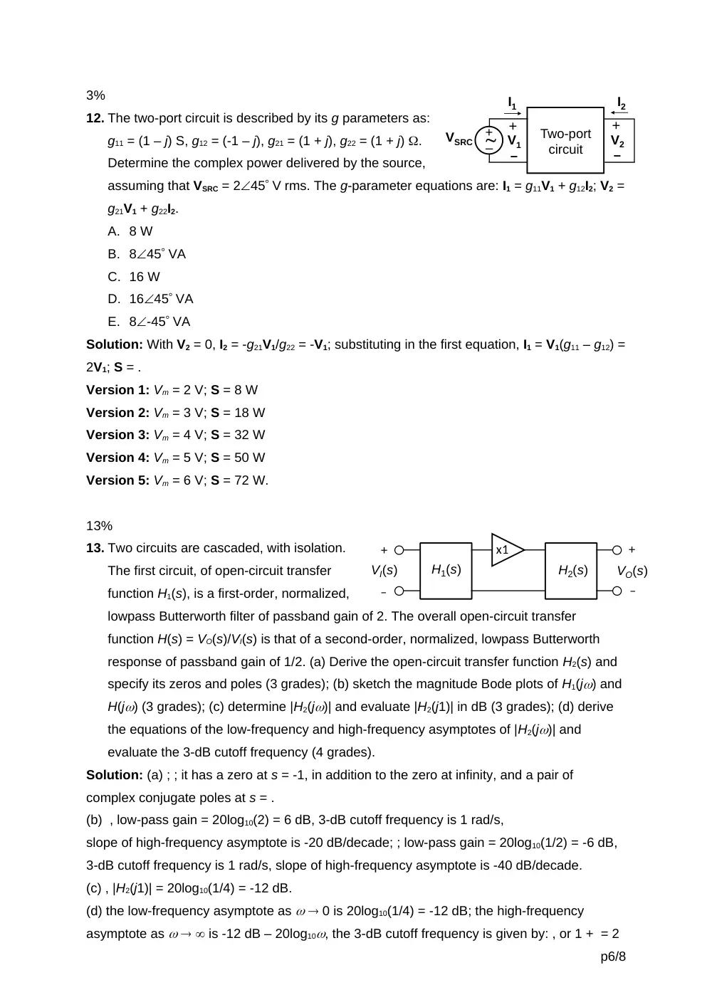
12. The two-port circuit is described by its g parameters as:
g11 = (1 – j) S, g12 = (-1 – j), g21 = (1 + j), g22 = (1 + j) .
Determine the complex power delivered by the source,
assuming that VSRC = 245 V rms. The g-parameter equations are: I1 = g11V1 + g12I2; V2 =
g21V1 + g22I2.
A. 8 W
B. 845 VA
C. 16 W
D. 1645 VA
E. 8-45 VA
Solution: With V2 = 0, I2 = -g21V1/g22 = -V1; substituting in the first equation, I1 = V1(g11 – g12) =
2V1; S = .
Version 1: Vm = 2 V; S = 8 W
Version 2: Vm = 3 V; S = 18 W
Version 3: Vm = 4 V; S = 32 W
Version 4: Vm = 5 V; S = 50 W
Version 5: Vm = 6 V; S = 72 W.
13%
13. Two circuits are cascaded, with isolation.
The first circuit, of open-circuit transfer
function H1(s), is a first-order, normalized,
lowpass Butterworth filter of passband gain of 2. The overall open-circuit transfer
function H(s) = VO(s)/VI(s) is that of a second-order, normalized, lowpass Butterworth
response of passband gain of 1/2. (a) Derive the open-circuit transfer function H2(s) and
specify its zeros and poles (3 grades); (b) sketch the magnitude Bode plots of H1(j) and
H(j) (3 grades); (c) determine |H2(j)| and evaluate |H2(j1)| in dB (3 grades); (d) derive
the equations of the low-frequency and high-frequency asymptotes of |H2(j)| and
evaluate the 3-dB cutoff frequency (4 grades).
Solution: (a) ; ; it has a zero at s = -1, in addition to the zero at infinity, and a pair of
complex conjugate poles at s = .
(b) , low-pass gain = 20log10(2) = 6 dB, 3-dB cutoff frequency is 1 rad/s,
slope of high-frequency asymptote is -20 dB/decade; ; low-pass gain = 20log10(1/2) = -6 dB,
3-dB cutoff frequency is 1 rad/s, slope of high-frequency asymptote is -40 dB/decade.
(c) , |H2(j1)| = 20log10(1/4) = -12 dB.
(d) the low-frequency asymptote as 0 is 20log10(1/4) = -12 dB; the high-frequency
asymptote as is -12 dB – 20log10, the 3-dB cutoff frequency is given by: , or 1 + = 2
p6/8
t, s
T
T
3T
5T
5T 3T
f(t)
1
5 F
2 mH
+
–
32 V
32
t = 0
+
–
vC
1/sC
sL
32/s
32
I(s)
–
+
–
+
L
+
–
VC(s)
500
turns
1000
turns
- j 4
4
–
+
100 V
rms
ZL
9
- j 9
–
+
150 V
rms
ZL
9
9
+ 2 , or – 2 – 1 = 0, which gives , or c = 1.55 rad/s.
13%
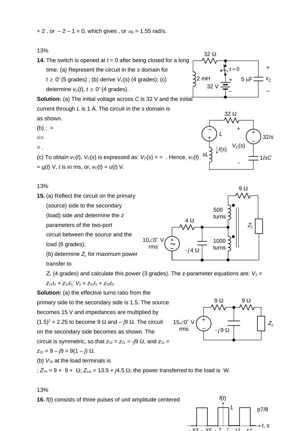
14. The switch is opened at t = 0 after being closed for a long
time. (a) Represent the circuit in the s domain for
t 0+ (5 grades) ; (b) derive VC(s) (4 grades); (c)
determine vC(t), t 0+ (4 grades).
Solution: (a) The initial voltage across C is 32 V and the initial
current through L is 1 A. The circuit in the s domain is
as shown.
(b) ; =
==
= .
(c) To obtain vC(t), VC(s) is expressed as: VC(s) = = . Hence, vC(t)
= u(t) V, t is in ms, or, vC(t) = u(t) V.
13%
15. (a) Reflect the circuit on the primary
(source) side to the secondary
(load) side and determine the z
parameters of the two-port
circuit between the source and the
load (6 grades);
(b) determine ZL for maximum power
transfer to
ZL (4 grades) and calculate this power (3 grades). The z-parameter equations are: V1 =
z11I1 + z12I2; V2 = z21I1 + z22I2.
Solution: (a) the effective turns ratio from the
primary side to the secondary side is 1.5. The source
becomes 15 V and impedances are multiplied by
(1.5)2 = 2.25 to become 9 and – j9 . The circuit
on the secondary side becomes as shown. The
circuit is symmetric, so that z12 = z21 = -j9 , and z11 =
z22 = 9 – j9 = 9(1 – j) .
(b) VTh at the load terminals is
; ZTh = 9 + 9 + ; ZLm = 13.5 + j4.5 ; the power transferred to the load is W.
13%
16. f(t) consists of three pulses of unit amplitude centered
p7/8
at the origin, each pulse being of duration T/2 and
separated from the adjacent pulse by T/2. It is required
to derive the convolution function y(t) = f(t)cos using the convolution-in-time property of
the Fourier transform.
Solution: The FT of the middle pulse is . Adding a delayed pulse and an advanced pulse
gives: = . Multiplying by the FT of cos: . This product is non-zero only at . The term is even
in and evaluates at to . The product of the two FTs becomes: = . This is the FT of y(t). It
follows that y(t) = . Check: direct application of the convolution integral gives the same result:
+ + .
p8/8