
EECE 310 Problems BJT Problems (No Answers), Fall 2013
American University of Beirut · Electronics · 8 pages · with solution

More EECE 310 files
- Questions Spice 3 Problem · Summer 2012ProblemsView
- Problems For BJT · Fall 2010ProblemsView
- Lecture Slides of Chapter 15 · Summer 2019LabView
- Lecture Slides of Chapter 12 · Summer 2019LabView
- Lecture Slides of Chapter 16 · Summer 2019LabView
- Lecture Slides of Chapter 14 · Summer 2019LabView
- Lecture Slides of Chapter 13 · Summer 2019LabView
- Lecture Slides of Chapter 17 · Summer 2019LabView
Show the text of this problems
EECE 310 – SAMPLE BJT PROBLEMS
�
Unless otherwise specified, assume that:
�
VT = 25 mV
�
|VBE(ACTIVE)| = 0.7 V
�
|VCE(SAT)| = 0.2 V
�
� = 100
�
Capacitors are very large
�
Body effect, Early effect, and channel-length modulation are negligible
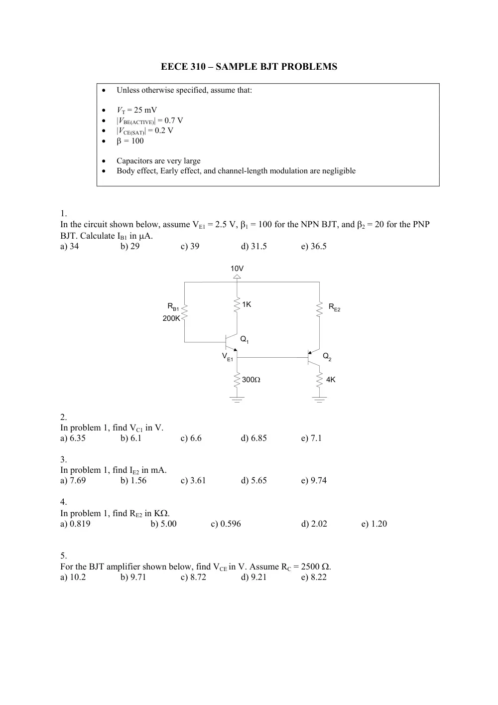
1.
In the circuit shown below, assume VE1 = 2.5 V, �1 = 100 for the NPN BJT, and �2 = 20 for the PNP
BJT. Calculate IB1 in �A.
a) 34
b) 29
c) 39
d) 31.5
e) 36.5
300�
1K
10V
4K
RE2
RB1
Q1
Q2
200K
VE1
2.
In problem 1, find VC1 in V.
a) 6.35
b) 6.1
c) 6.6
d) 6.85
e) 7.1
3.
In problem 1, find IE2 in mA.
a) 7.69
b) 1.56
c) 3.61
d) 5.65
e) 9.74
4.
In problem 1, find RE2 in K�.
a) 0.819
b) 5.00
c) 0.596
d) 2.02
e) 1.20
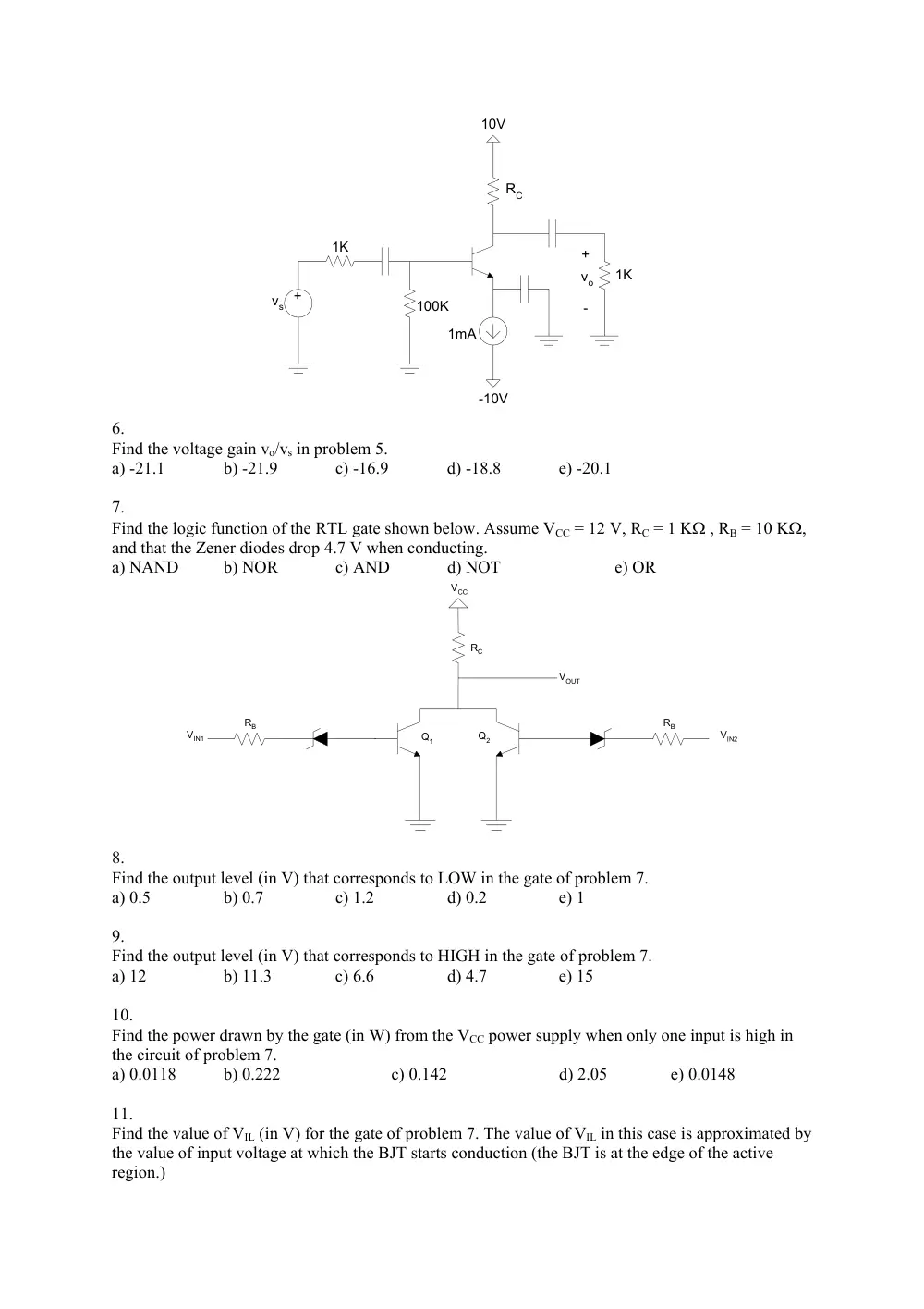
5.
For the BJT amplifier shown below, find VCE in V. Assume RC = 2500 �.
a) 10.2
b) 9.71
c) 8.72
d) 9.21
e) 8.22
10V
-10V
1mA
1K
100K
1K
vo
+
-
vs +
RC
6.
Find the voltage gain vo/vs in problem 5.
a) -21.1
b) -21.9
c) -16.9
d) -18.8
e) -20.1
7.
Find the logic function of the RTL gate shown below. Assume VCC = 12 V, RC = 1 K� , RB = 10 K�,
and that the Zener diodes drop 4.7 V when conducting.
a) NAND
b) NOR
c) AND
d) NOT
e) OR
VCC
VOUT
VIN2
VIN1
RC
RB
RB
Q1
Q2
8.
Find the output level (in V) that corresponds to LOW in the gate of problem 7.
a) 0.5
b) 0.7
c) 1.2
d) 0.2
e) 1
9.
Find the output level (in V) that corresponds to HIGH in the gate of problem 7.
a) 12
b) 11.3
c) 6.6
d) 4.7
e) 15
10.
Find the power drawn by the gate (in W) from the VCC power supply when only one input is high in
the circuit of problem 7.
a) 0.0118
b) 0.222
c) 0.142
d) 2.05
e) 0.0148
11.
Find the value of VIL (in V) for the gate of problem 7. The value of VIL in this case is approximated by
the value of input voltage at which the BJT starts conduction (the BJT is at the edge of the active
region.)
a) 0.7
b) 5.4
c) 1.4
d) 12
e) 4.7 V
12.
Find the base current of Q1 (in mA) in the circuit of problem 7, when Q1 is at the edge of the
saturation region. Assume that VIN2 is low.
a) 0.841
b) 0.075
c) 0.118
d) 0.148
e) 0.536
13.
Find the value of VIH (in V) for the gate of problem 7. The value of VIH in this case is approximated
by the value of input voltage at which the BJT is at the edge of saturation.
a) 6.58
b) 5.58
c) 6.88
d) 5.88
e) 8.55
14.
Find the base current of Q1 (in mA) in the gate of problem 7 when the input voltage is VIN1 = 7 V.
Assume that VIN2 is low.
a) 0.06
b) 0.16
c) 0.26
d) 0.36
e) 0.46
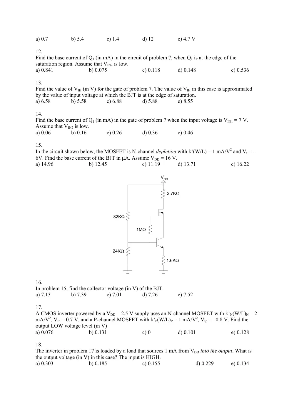
15.
In the circuit shown below, the MOSFET is N-channel depletion with k’(W/L) = 1 mA/V2 and Vt = –
6V. Find the base current of the BJT in �A. Assume VDD = 16 V.
a) 14.96
b) 12.45
c) 11.19
d) 13.71
e) 16.22
VDD
1M�
24K�
82K�
2.7K�
1.6K�
16.
In problem 15, find the collector voltage (in V) of the BJT.
a) 7.13
b) 7.39
c) 7.01
d) 7.26
e) 7.52
17.
A CMOS inverter powered by a VDD = 2.5 V supply uses an N-channel MOSFET with k’N(W/L)N = 2
mA/V2, Vtn = 0.7 V, and a P-channel MOSFET with k’P(W/L)P = 1 mA/V2, Vtp = –0.8 V. Find the
output LOW voltage level (in V)
a) 0.076
b) 0.131
c) 0
d) 0.101
e) 0.128
18.
The inverter in problem 17 is loaded by a load that sources 1 mA from VDD into the output. What is
the output voltage (in V) in this case? The input is HIGH.
a) 0.303
b) 0.185
c) 0.155
d) 0.229
e) 0.134
19.
What is the dynamic power dissipation (in mW) of the CMOS inverter in problem 17 when it is
loaded by a 1 pF capacitor and its input is a 16 MHz clock.
a) 0.324
b) 0.1
c) 0.256
d) 0.144
e) 0.196
20.
The propagation delay of the CMOS inverter in problem 17 is 1 ns when loaded by a 1 pF capacitor.
What happens to the propagation delay when the load capacitance is reduced to 0.5 pF? The delay is
a) unchanged
b) increased to 2ns
c) reduced to 0.5 ns
d) increased to 4 ns
e) reduced to 0.25 ns
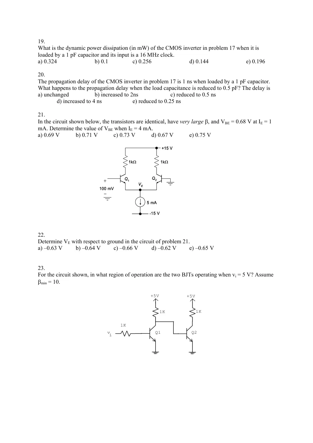
21.
In the circuit shown below, the transistors are identical, have very large �, and VBE = 0.68 V at IE = 1
mA. Determine the value of VBE when IE = 4 mA.
a) 0.69 V
b) 0.71 V
c) 0.73 V
d) 0.67 V
e) 0.75 V
22.
Determine VE with respect to ground in the circuit of problem 21.
a) –0.63 V
b) –0.64 V
c) –0.66 V
d) –0.62 V
e) –0.65 V
23.
For the circuit shown, in what region of operation are the two BJTs operating when vi = 5 V? Assume
�min = 10.
1K
+5V
1K
vi
+5V
1K
Q2
Q1
1k�
+15 V
5 mA
Q1
Q2
-15 V
1k�
+
–
VE
100 mV
1k�
+15 V
5 mA
Q1
Q2
-15 V
1k�
+
–
VE
100 mV
24.
In the circuit shown below, assume � = 99.
a) Find the base current of the BJT.
b) Find the value of VCE.
10K
+10V
-10V
100K
560K
25.
A 10 K� resistor is connected between the output of a CMOS inverter and ground. Find the resulting
value of VOH (when the input is zero volts.) Assume VDD = 5 V, Vtn = -Vtp = 1 V, and k’n(W/L)n = k’p
(W/L)p = 0.1 mA/V2.
26.
Refer to the circuit shown on the right. Determine R so that the DC
output VO = 2 V, assuming � to be very large, VBE = 0.8 V, k’n(W/L) =
0.2 mA / V2, and Vt = 1 V.
a) 4.36 M�
b) 3.17 M�
c) 10.54 M�
d) 6.14 M�
e) none of the above
27.
In the previous problem, find the collector current of the BJT.
a) 1.5 mA b) 0.5 mA c) 1.1 mA d) 2.1 mA e) none of the above
VO
+
+5 V
–
2 k�
2 k�
1 M�
R
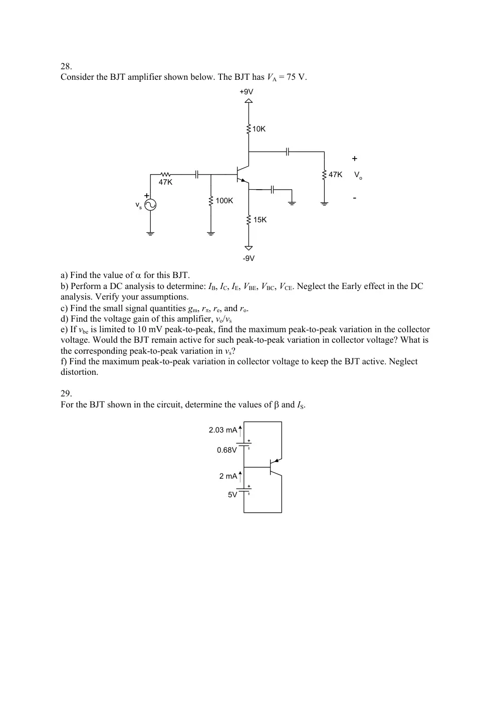
28.
Consider the BJT amplifier shown below. The BJT has VA = 75 V.
47K
Vo
+
-
+9V
-9V
10K
100K
15K
vs
+
47K
a) Find the value of � for this BJT.
b) Perform a DC analysis to determine: IB, IC, IE, VBE, VBC, VCE. Neglect the Early effect in the DC
analysis. Verify your assumptions.
c) Find the small signal quantities gm, r�, re, and ro.
d) Find the voltage gain of this amplifier, vo/vs
e) If vbe is limited to 10 mV peak-to-peak, find the maximum peak-to-peak variation in the collector
voltage. Would the BJT remain active for such peak-to-peak variation in collector voltage? What is
the corresponding peak-to-peak variation in vs?
f) Find the maximum peak-to-peak variation in collector voltage to keep the BJT active. Neglect
distortion.
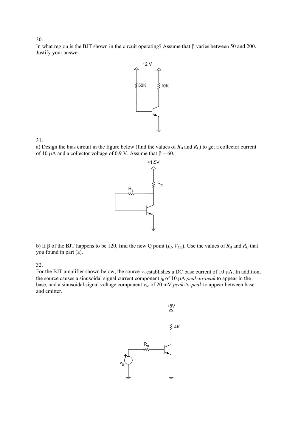
29.
For the BJT shown in the circuit, determine the values of � and IS.
0.68V
5V
2 mA
2.03 mA
30.
In what region is the BJT shown in the circuit operating? Assume that � varies between 50 and 200.
Justify your answer.
10K
50K
12 V
31.
a) Design the bias circuit in the figure below (find the values of RB and RC) to get a collector current
of 10 �A and a collector voltage of 0.9 V. Assume that � = 60.
+1.5V
RC
RB
b) If � of the BJT happens to be 120, find the new Q point (IC, VCE). Use the values of RB and RC that
you found in part (a).
32.
For the BJT amplifier shown below, the source vS establishes a DC base current of 10 �A. In addition,
the source causes a sinusoidal signal current component ib of 10 �A peak-to-peak to appear in the
base, and a sinusoidal signal voltage component vbe of 20 mV peak-to-peak to appear between base
and emitter.
4K
vS
+
+8V
RB
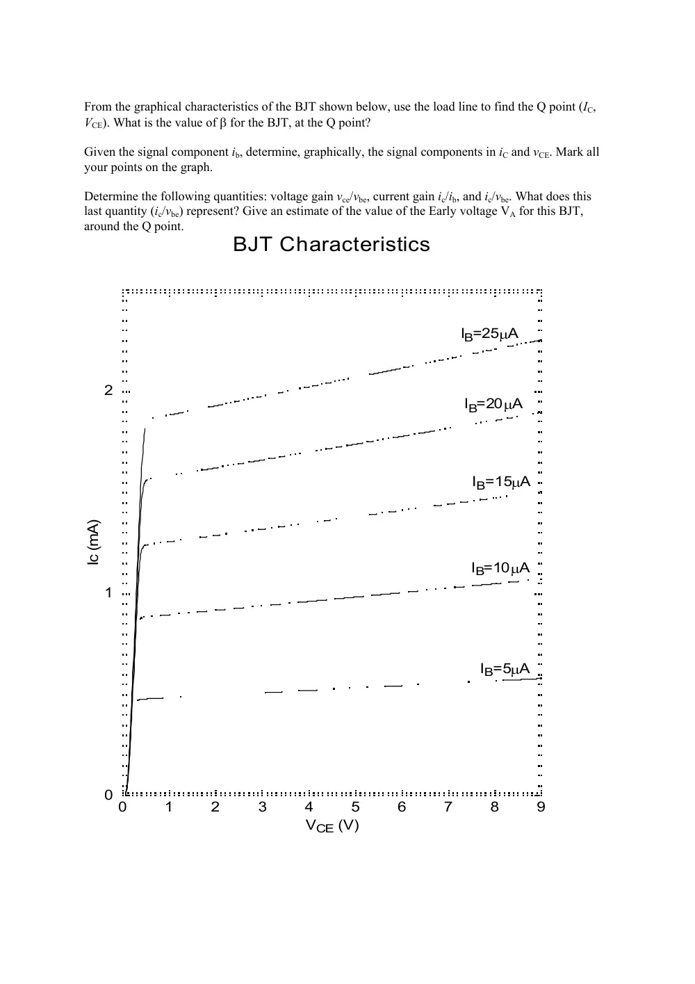
From the graphical characteristics of the BJT shown below, use the load line to find the Q point (IC,
VCE). What is the value of � for the BJT, at the Q point?
Given the signal component ib, determine, graphically, the signal components in iC and vCE. Mark all
your points on the graph.
Determine the following quantities: voltage gain vce/vbe, current gain ic/ib, and ic/vbe. What does this
last quantity (ic/vbe) represent? Give an estimate of the value of the Early voltage VA for this BJT,
around the Q point.
0
1
2
3
4
5
6
7
8
9
VCE (V)
0
1
2
Ic (mA)
BJT Characteristics
IB=5�A
IB=10�A
IB=15�A
IB=20�A
IB=25�A