
EECE 310L Lab 7, Fall 2011
American University of Beirut · Electric Circuits Laboratory · 7 pages

More EECE 310L files
Show the text of this lab
EECE 310L : Electric Circuits Laboratory
Experiment 7
1
A m e r i c a n U n i v e r s i t y o f B e i r u t
Fall 2011
Experiment 7
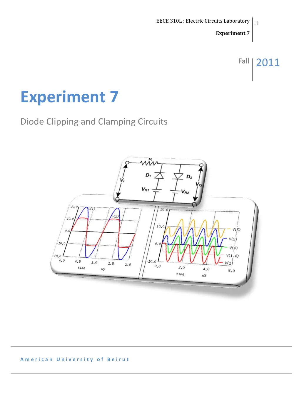
Diode Clipping and Clamping Circuits
EECE 310L : Electric Circuits Laboratory
Experiment 7
2
Table of Contents
I.
Objectives .................................................................................................................................. 3
II.
Material and Procedure ........................................................................................................ 3
A.
Diode clipping and clamping circuits ......................................................................... 3
A1.
One diode clipping Circuit .................................................................................................. 3
A2.
Zener diodes clipping circuit ............................................................................................. 3
A3.
Clampping circuit application 1 ....................................................................................... 4
A4.
Clampping circuit application 2 ....................................................................................... 5
A5.
ClaMpping circuit application 3........................................................................................ 5
III. Outcomes ................................................................................................................................... 7
EECE 310L : Electric Circuits Laboratory
Experiment 7
3
I.
OBJECTIVES
In this experiment you will:
Investigate the diode clipping circuits, their characteristics and applications
Investigate the diode clamping circuits, their characteristics and applications
II. MATERIAL AND PROCEDURE
Procedure
A. DIODE CLIPPING AND CLAMPING CIRCUITS
A1. ONE DIODE CLIPPING CIRCUIT
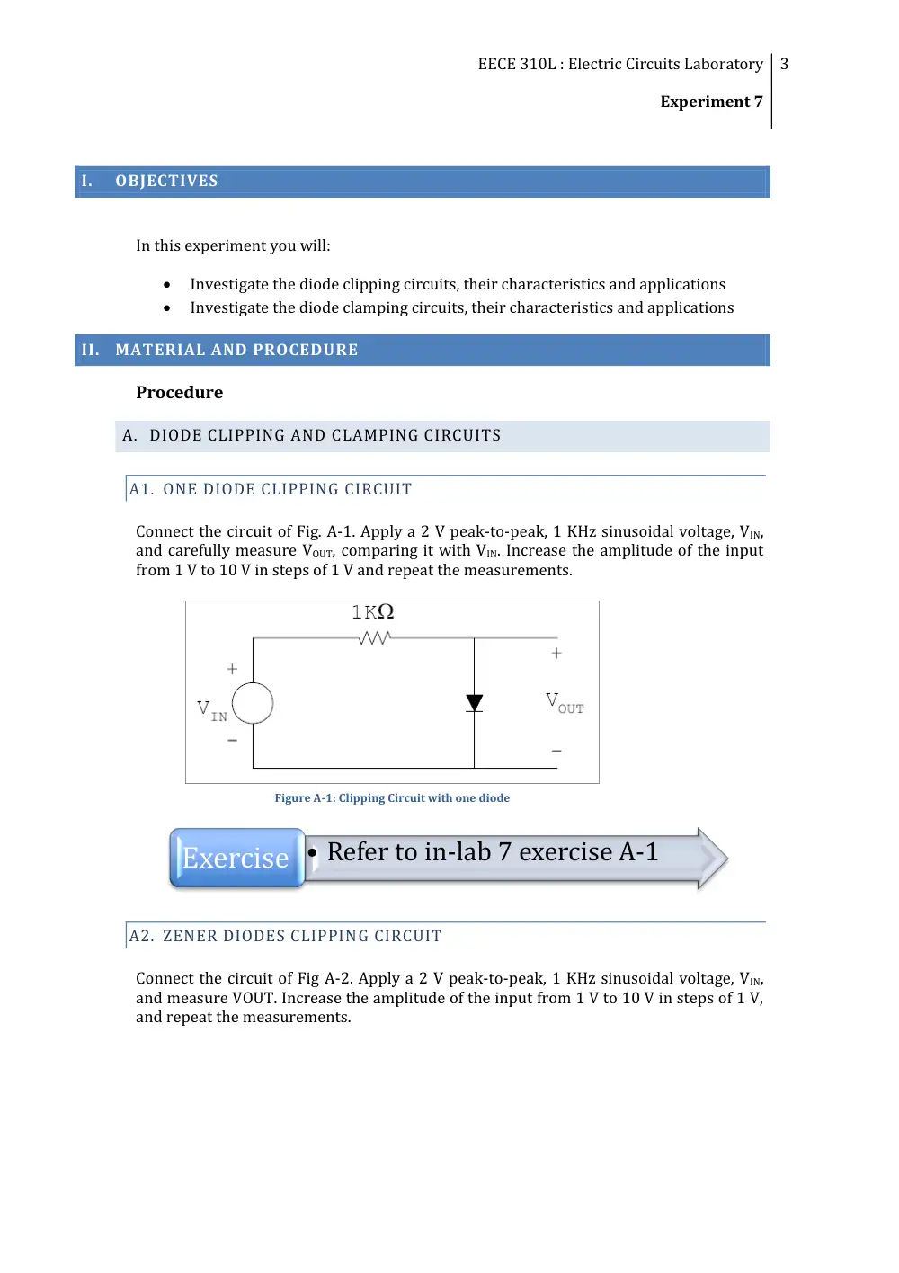
Connect the circuit of Fig. A-1. Apply a 2 V peak-to-peak, 1 KHz sinusoidal voltage, VIN,
and carefully measure VOUT, comparing it with VIN. Increase the amplitude of the input
from 1 V to 10 V in steps of 1 V and repeat the measurements.
A2. ZENER DIODES CLIPPING CIRCUIT
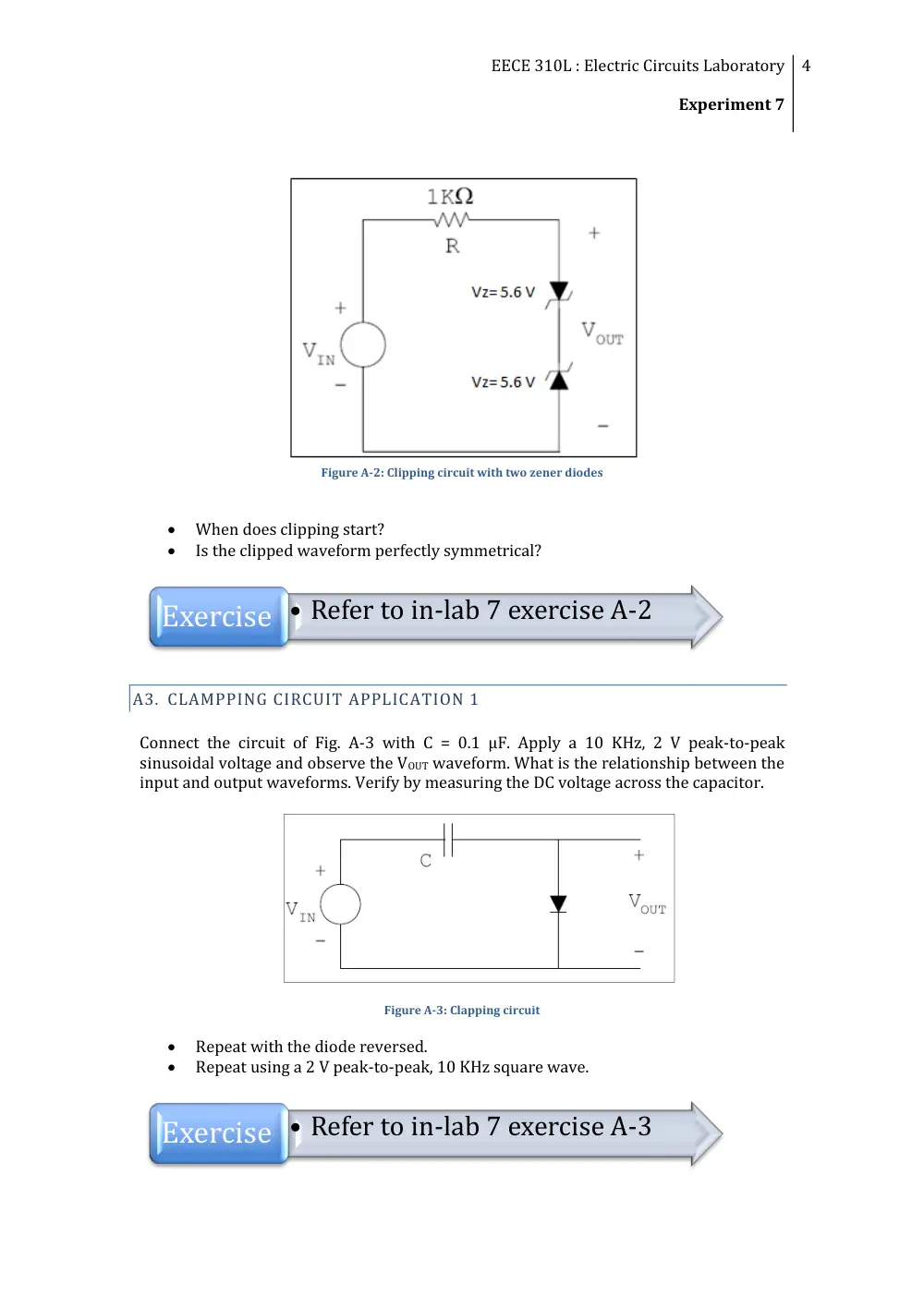
Connect the circuit of Fig A-2. Apply a 2 V peak-to-peak, 1 KHz sinusoidal voltage, VIN,
and measure VOUT. Increase the amplitude of the input from 1 V to 10 V in steps of 1 V,
and repeat the measurements.
• Refer to in-lab 7 exercise A-1
Exercise
Figure A-1: Clipping Circuit with one diode
EECE 310L : Electric Circuits Laboratory
Experiment 7
4
Figure A-2: Clipping circuit with two zener diodes
When does clipping start?
Is the clipped waveform perfectly symmetrical?
A3. CLAMPPING CIRCUIT APPLICATION 1
Connect the circuit of Fig. A-3 with C = 0.1 µF. Apply a 10 KHz, 2 V peak-to-peak
sinusoidal voltage and observe the VOUT waveform. What is the relationship between the
input and output waveforms. Verify by measuring the DC voltage across the capacitor.
Figure A-3: Clapping circuit
Repeat with the diode reversed.
Repeat using a 2 V peak-to-peak, 10 KHz square wave.
• Refer to in-lab 7 exercise A-2
Exercise
Exercise • Refer to in-lab 7 exercise A-3
EECE 310L : Electric Circuits Laboratory
Experiment 7
5
A4. CLAMPPING CIRCUIT APPLICATION 2
Connect a 10 KΩ resistor in parallel with the diode in Fig. A-3, and measure the DC shift
of VOUT.
Repeat with a 1 KΩ resistor. Explain the effect of the load resistor on the DC shift.
A5. CLAMPPING CIRCUIT APPLICATION 3
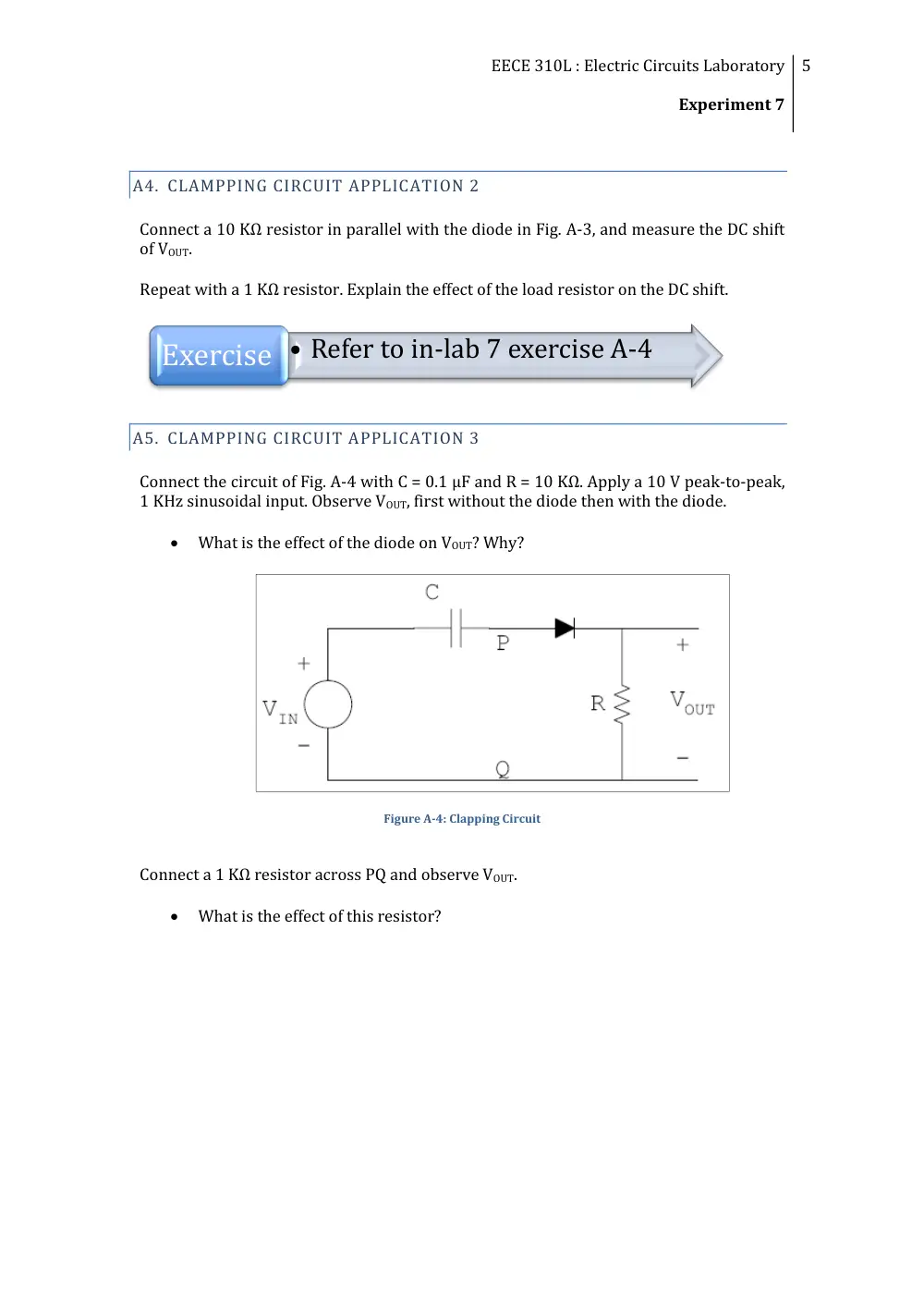
Connect the circuit of Fig. A-4 with C = 0.1 µF and R = 10 KΩ. Apply a 10 V peak-to-peak,
1 KHz sinusoidal input. Observe VOUT, first without the diode then with the diode.
What is the effect of the diode on VOUT? Why?
Figure A-4: Clapping Circuit
Connect a 1 KΩ resistor across PQ and observe VOUT.
What is the effect of this resistor?
• Refer to in-lab 7 exercise A-4
Exercise
EECE 310L : Electric Circuits Laboratory
Experiment 7
6
Discussion on Part A
•
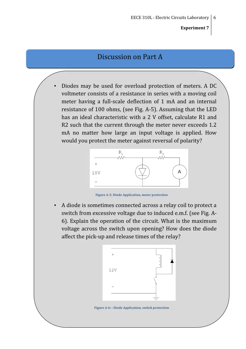
Diodes may be used for overload protection of meters. A DC
voltmeter consists of a resistance in series with a moving coil
meter having a full-scale deflection of 1 mA and an internal
resistance of 100 ohms, (see Fig. A-5). Assuming that the LED
has an ideal characteristic with a 2 V offset, calculate R1 and
R2 such that the current through the meter never exceeds 1.2
mA no matter how large an input voltage is applied. How
would you protect the meter against reversal of polarity?
Figure A-5: Diode Application, meter protection
•
A diode is sometimes connected across a relay coil to protect a
switch from excessive voltage due to induced e.m.f. (see Fig. A-
6). Explain the operation of the circuit. What is the maximum
voltage across the switch upon opening? How does the diode
affect the pick-up and release times of the relay?
Figure A-6: : Diode Application, switch protection
EECE 310L : Electric Circuits Laboratory
Experiment 7
7
III.
OUTCOMES
By the end of Experiment VII, students:
Are familiar with diode clipping circuits, their characteristics and applications
Are familiar with diode clamping circuits, their characteristics and applications
•
Modify the circuit of Fig. A-2 so as to have symmetrical clipping,
using a single Zener diode and a diode bridge.
•
For effective clamping in Fig. A-3, what should be the
relationship between the period of the applied waveform and
the RC time constant?
•
The circuit in Fig. A-7 illustrates a voltage multiplying rectifier
circuit. Assuming ideal diodes, trace the peak charging voltage
across the capacitors. Compare the voltages across AC, AD, BE
and BF with the peak value of VIN.
Figure A-7: Voltage Multiplier
Discussion on Part A