
EECE 310L Lab 8, Fall 2011
American University of Beirut · Electric Circuits Laboratory · 10 pages
More EECE 310L files
Show the text of this lab
EECE 310L : Electric Circuits Laboratory
Experiment 8
1
A m e r i c a n U n i v e r s i t y o f B e i r u t
Fall 2011
Experiment 8
Op‐Amp Circuits
EECE 310L : Electric Circuits Laboratory
Experiment 8
2
Table of Contents
I.
Objectives ................................................................................................................................ 3
II.
Material and Procedure ...................................................................................................... 3
A.
Inverting Amplifier .......................................................................................................... 3
A1.
Inverting amplifier procedure 1: Theoretical Vs measured .................................. 3
A2.
Inverting amplifier procedure 2: BAndwidth ............................................................... 4
A3.
Inverting amplifier procedure 3: High Input ................................................................ 4
B.
NonInverting Amplifier ................................................................................................ 5
B1.
non‐Inverting amplifier procedure 1: Theoretical Vs measured ........................ 5
B2.
non‐Inverting amplifier procedure 2: BAndwidth ..................................................... 6
C.
UnityGain NonInverting Amplifier........................................................................... 6
C1.
Unity amplifier procedure ..................................................................................................... 6
D.
Inverting Adder ................................................................................................................ 7
E.
Integrator ........................................................................................................................... 8
E1.
Integrator: theoretical calculation ..................................................................................... 8
E2.
Integrator: Theoretical vs measured ................................................................................ 8
E3.
Integrator: Bandwidth ............................................................................................................. 9
F.
Differentiator .................................................................................................................... 9
F1.
differentiator: theoretical calculation ........................................................................... 10
F2.
Integrator: Theoretical vs measured ............................................................................. 10
III. Outcomes .............................................................................................................................. 10
EECE 310L : Electric Circuits Laboratory
Experiment 8
3
I.
OBJECTIVES
In this experiment you will investigate the characteristics of the following op‐amp
circuits:
•
inverting amplifier
•
non‐inverting amplifier
•
unit‐gain buffer
•
inverting adder
•
integrator
•
differentiator
II. MATERIAL AND PROCEDURE
A. INVERTING AMPLIFIER
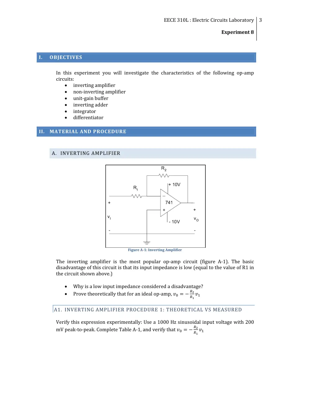
Figure A1: Inverting Amplifier
The inverting amplifier is the most popular op‐amp circuit (figure A‐1). The basic
disadvantage of this circuit is that its input impedance is low (equal to the value of R1 in
the circuit shown above.)
•
Why is a low input impedance considered a disadvantage?
•
Prove theoretically that for an ideal op‐amp, �� � �
��
�� ��
A1. INVERTING AMPLIFIER PROCEDURE 1: THEORETICAL VS MEASURED
Verify this expression experimentally: Use a 1000 Hz sinusoidal input voltage with 200
mV peak‐to‐peak. Complete Table A‐1, and verify that �� � �
��
�� ��
EECE 310L : Electric Circuits Laboratory
Experiment 8
4
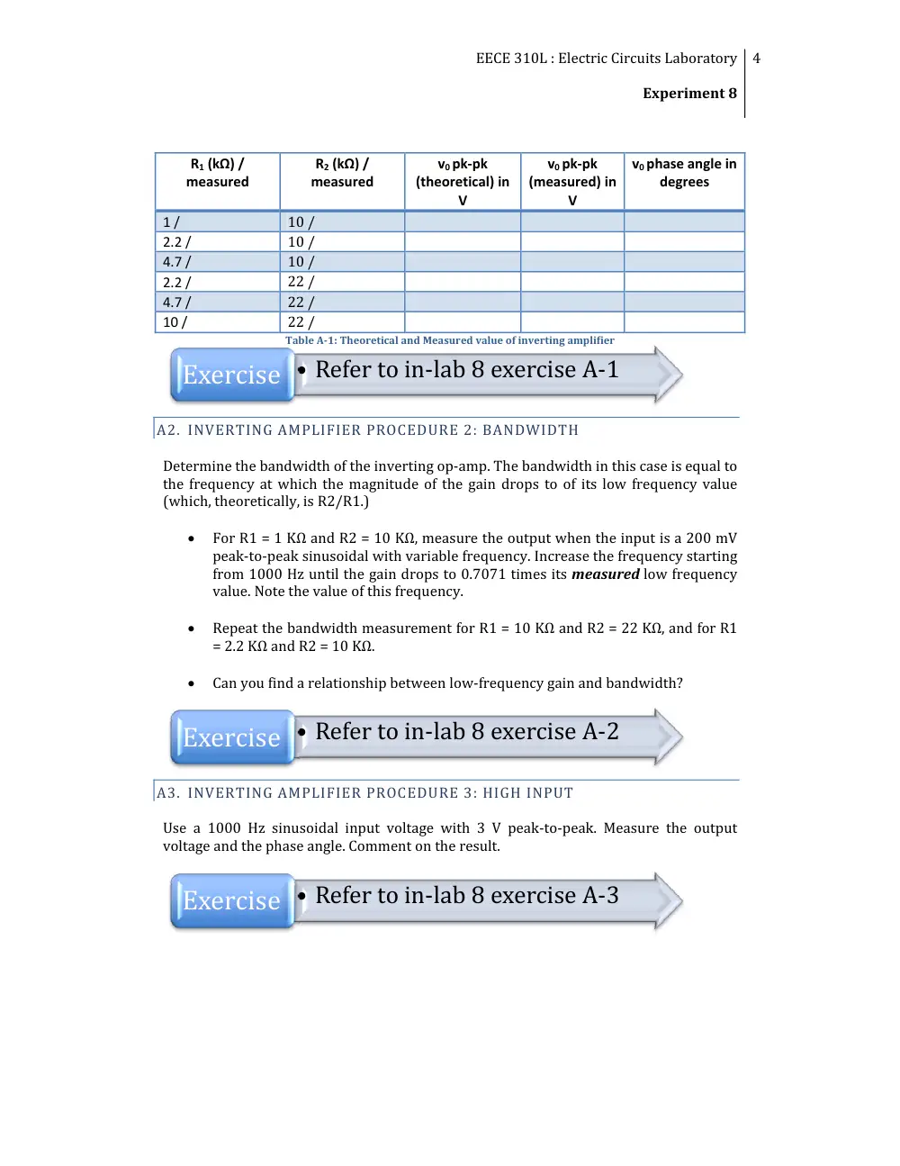
R1 (kΩ) /
measured
R2 (kΩ) /
measured
v0 pk‐pk
(theoretical) in
V
v0 pk‐pk
(measured) in
V
v0 phase angle in
degrees
1 /
10 /
2.2 /
10 /
4.7 /
10 /
2.2 /
22 /
4.7 /
22 /
10 /
22 /
Table A1: Theoretical and Measured value of inverting amplifier
A2. INVERTING AMPLIFIER PROCEDURE 2: BANDWIDTH
Determine the bandwidth of the inverting op‐amp. The bandwidth in this case is equal to
the frequency at which the magnitude of the gain drops to of its low frequency value
(which, theoretically, is R2/R1.)
•
For R1 = 1 KΩ and R2 = 10 KΩ, measure the output when the input is a 200 mV
peak‐to‐peak sinusoidal with variable frequency. Increase the frequency starting
from 1000 Hz until the gain drops to 0.7071 times its measured low frequency
value. Note the value of this frequency.
•
Repeat the bandwidth measurement for R1 = 10 KΩ and R2 = 22 KΩ, and for R1
= 2.2 KΩ and R2 = 10 KΩ.
•
Can you find a relationship between low‐frequency gain and bandwidth?
A3. INVERTING AMPLIFIER PROCEDURE 3: HIGH INPUT
Use a 1000 Hz sinusoidal input voltage with 3 V peak‐to‐peak. Measure the output
voltage and the phase angle. Comment on the result.
• Refer to in‐lab 8 exercise A‐1
Exercise
• Refer to in‐lab 8 exercise A‐2
Exercise
Exercise • Refer to in‐lab 8 exercise A‐3
EECE 310L : Electric Circuits Laboratory
Experiment 8
5
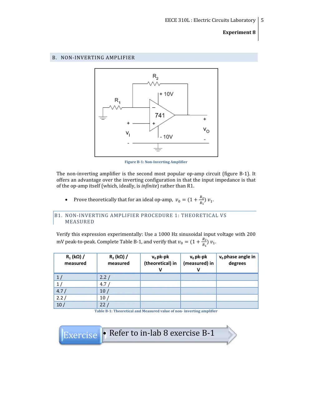
B. NON‐INVERTING AMPLIFIER
Figure B1: NonInverting Amplifier
The non‐inverting amplifier is the second most popular op‐amp circuit (figure B‐1). It
offers an advantage over the inverting configuration in that the input impedance is that
of the op‐amp itself (which, ideally, is infinite) rather than R1.
•
Prove theoretically that for an ideal op‐amp, �� � �1 �
��
��� ��.
B1. NON‐INVERTING AMPLIFIER PROCEDURE 1: THEORETICAL VS
MEASURED
Verify this expression experimentally: Use a 1000 Hz sinusoidal input voltage with 200
mV peak‐to‐peak. Complete Table B‐1, and verify that �� � �1 �
��
��� ��.
R1 (kΩ) /
measured
R2 (kΩ) /
measured
v0 pk‐pk
(theoretical) in
V
v0 pk‐pk
(measured) in
V
v0 phase angle in
degrees
1 /
2.2 /
1 /
4.7 /
4.7 /
10 /
2.2 /
10 /
10 /
22 /
Table B1: Theoretical and Measured value of non inverting amplifier
Exercise • Refer to in‐lab 8 exercise B‐1
EECE 310L : Electric Circuits Laboratory
Experiment 8
6
B2. NON‐INVERTING AMPLIFIER PROCEDURE 2: BANDWIDTH
Determine the bandwidth of the non‐inverting op‐amp. As before, the bandwidth is
equal to the frequency at which the magnitude of the gain
��
��
drops to
�
√� of its low
frequency value (which, theoretically, is 1 �
��
��)
•
For R1 = 1 KΩ and R2 = 4.7 KΩ, measure the output when the input is a 200 mV
peak‐to‐peak sinusoidal with variable frequency. Increase the frequency starting
from 1000 Hz until the gain drops to 0.7071 times its measured low frequency
value. Note the value of this frequency.
•
Repeat the bandwidth measurement for R1 = 10 KΩ and R2 = 22 KΩ.
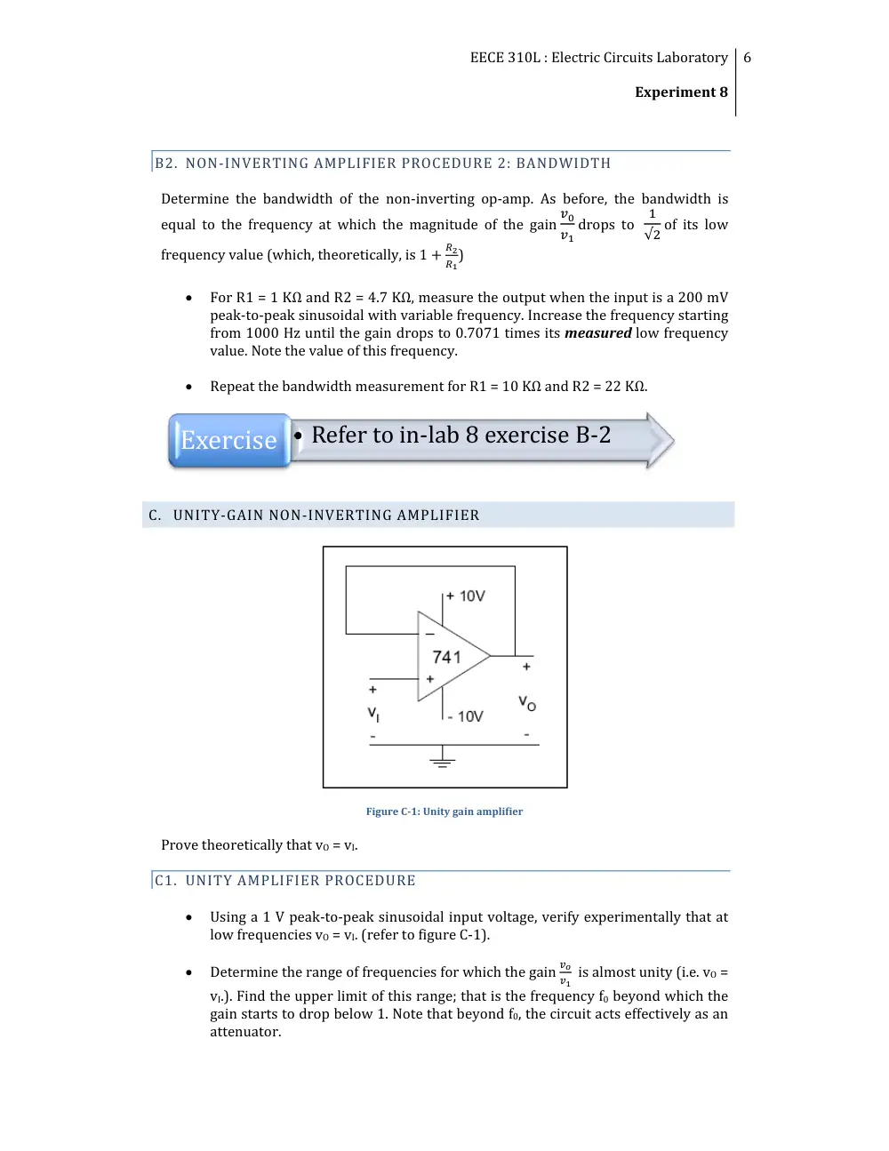
C. UNITY‐GAIN NON‐INVERTING AMPLIFIER
Figure C1: Unity gain amplifier
Prove theoretically that vO = vI.
C1. UNITY AMPLIFIER PROCEDURE
•
Using a 1 V peak‐to‐peak sinusoidal input voltage, verify experimentally that at
low frequencies vO = vI. (refer to figure C‐1).
•
Determine the range of frequencies for which the gain
��
�� is almost unity (i.e. vO =
vI.). Find the upper limit of this range; that is the frequency f0 beyond which the
gain starts to drop below 1. Note that beyond f0, the circuit acts effectively as an
attenuator.
Exercise • Refer to in‐lab 8 exercise B‐2
EECE 310L : Electric Circuits Laboratory
Experiment 8
7
•
Determine the bandwidth of the unity‐gain non‐inverting op‐amp. As before, the
bandwidth is equal to the frequency at which the magnitude of the gain
��
��
drops
to
�
√� (since the low‐frequency gain is theoretically equal to 1.)
•
How does this bandwidth compare with that of the non‐inverting amplifier?
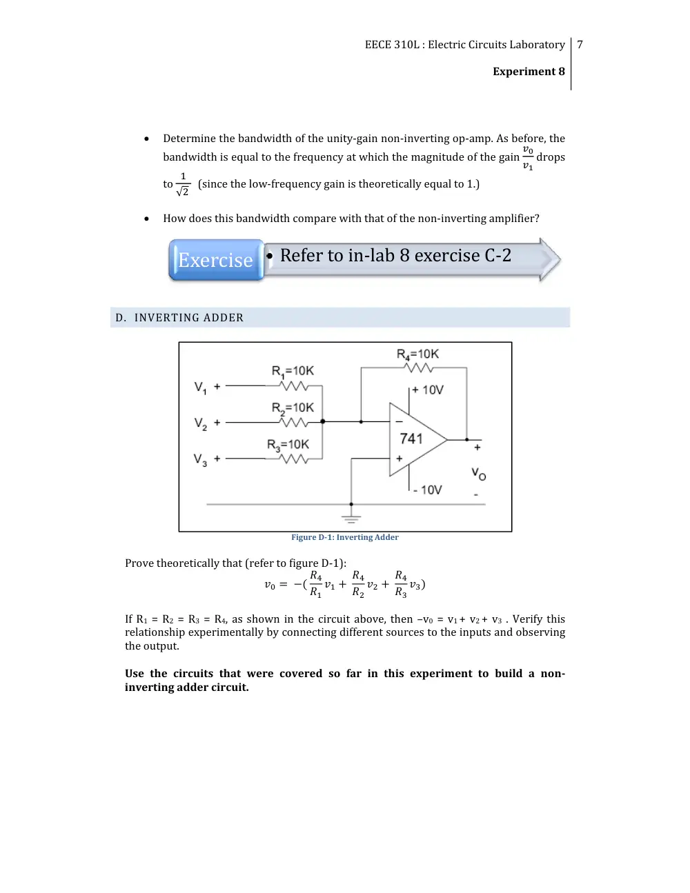
D. INVERTING ADDER
Figure D1: Inverting Adder
Prove theoretically that (refer to figure D‐1):
�� � �� ��
��
�� � ��
��
�� � ��
��
���
If R1 = R2 = R3 = R4, as shown in the circuit above, then –v0 = v1 + v2 + v3 . Verify this
relationship experimentally by connecting different sources to the inputs and observing
the output.
Use the circuits that were covered so far in this experiment to build a non
inverting adder circuit.
Exercise • Refer to in‐lab 8 exercise C‐2
EECE 310L : Electric Circuits Laboratory
Experiment 8
8
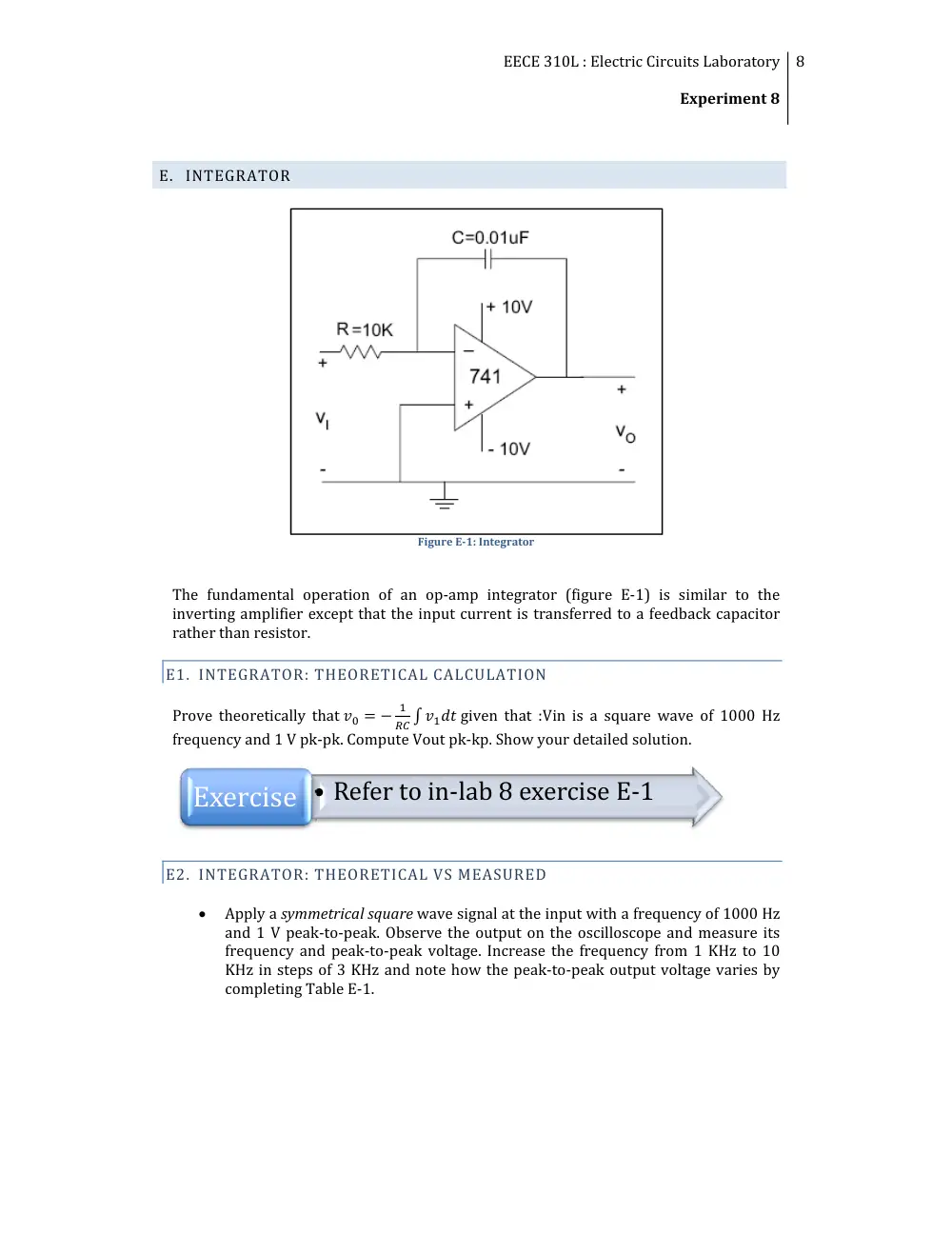
E. INTEGRATOR
Figure E1: Integrator
The fundamental operation of an op‐amp integrator (figure E‐1) is similar to the
inverting amplifier except that the input current is transferred to a feedback capacitor
rather than resistor.
E1. INTEGRATOR: THEORETICAL CALCULATION
Prove theoretically that �� � �
�
�� � ���� given that :Vin is a square wave of 1000 Hz
frequency and 1 V pk‐pk. Compute Vout pk‐kp. Show your detailed solution.
E2. INTEGRATOR: THEORETICAL VS MEASURED
•
Apply a symmetrical square wave signal at the input with a frequency of 1000 Hz
and 1 V peak‐to‐peak. Observe the output on the oscilloscope and measure its
frequency and peak‐to‐peak voltage. Increase the frequency from 1 KHz to 10
KHz in steps of 3 KHz and note how the peak‐to‐peak output voltage varies by
completing Table E‐1.
Exercise • Refer to in‐lab 8 exercise E‐1
EECE 310L : Electric Circuits Laboratory
Experiment 8
9
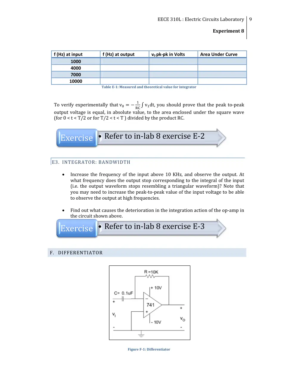
f (Hz) at input
f (Hz) at output
v0 pk‐pk in Volts
Area Under Curve
1000
4000
7000
10000
Table E1: Measured and theoretical value for integrator
To verify experimentally that v� � �
�
RC � v�dt, you should prove that the peak to‐peak
output voltage is equal, in absolute value, to the area enclosed under the square wave
(for 0 < t < T/2 or for T/2 < t < T ) divided by the product RC.
E3. INTEGRATOR: BANDWIDTH
•
Increase the frequency of the input above 10 KHz, and observe the output. At
what frequency does the output stop corresponding to the integral of the input
(i.e. the output waveform stops resembling a triangular waveform)? Note that
you may need to increase the peak‐to‐peak value of the input voltage to be able
to observe the output at high frequencies.
•
Find out what causes the deterioration in the integration action of the op‐amp in
the circuit shown above.
F. DIFFERENTIATOR
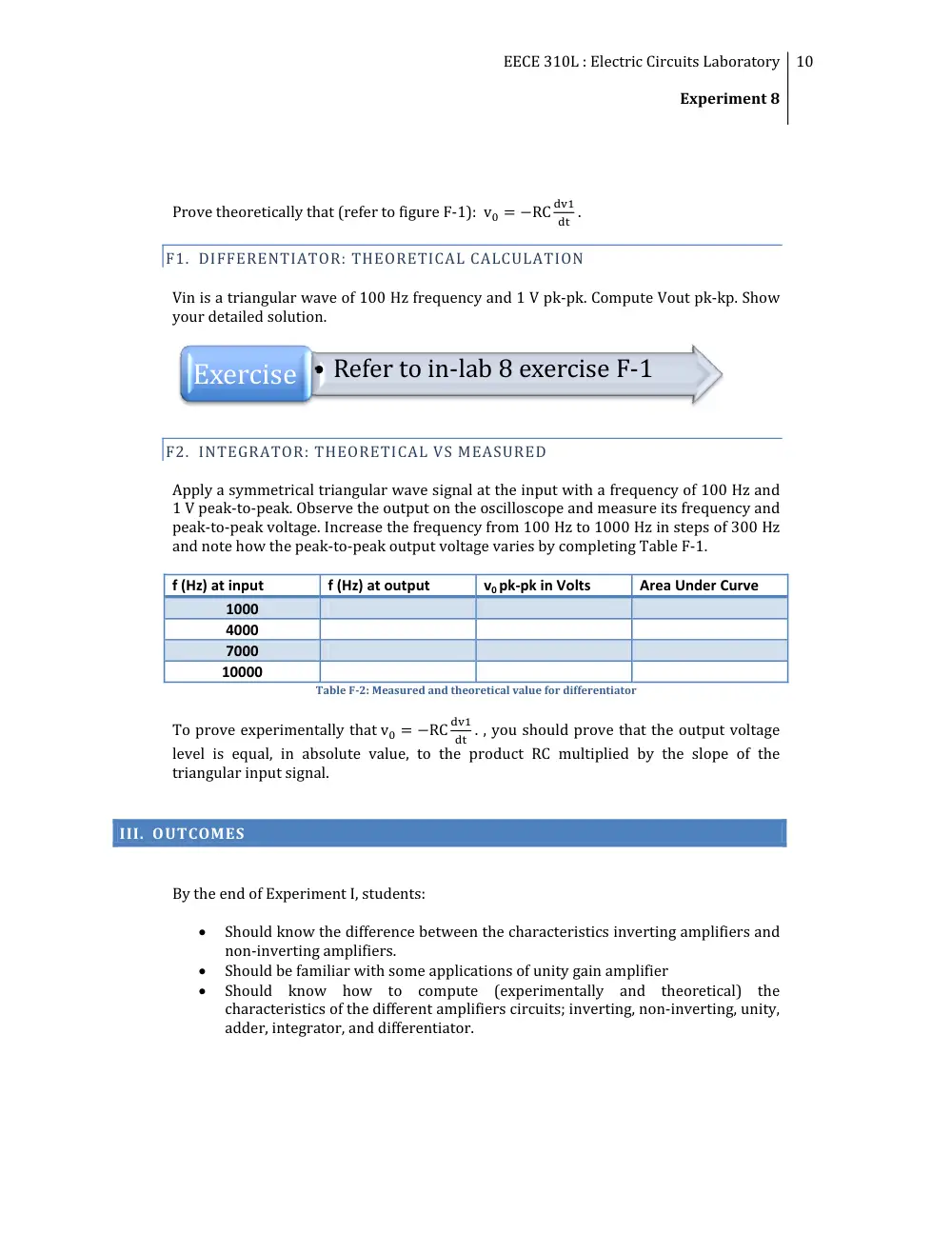
Figure F1: Differentiator
• Refer to in‐lab 8 exercise E‐2
Exercise
Exercise • Refer to in‐lab 8 exercise E‐3
EECE 310L : Electric Circuits Laboratory
Experiment 8
10
Prove theoretically that (refer to figure F‐1): v� � �RC
���
�� .
F1. DIFFERENTIATOR: THEORETICAL CALCULATION
Vin is a triangular wave of 100 Hz frequency and 1 V pk‐pk. Compute Vout pk‐kp. Show
your detailed solution.
F2. INTEGRATOR: THEORETICAL VS MEASURED
Apply a symmetrical triangular wave signal at the input with a frequency of 100 Hz and
1 V peak‐to‐peak. Observe the output on the oscilloscope and measure its frequency and
peak‐to‐peak voltage. Increase the frequency from 100 Hz to 1000 Hz in steps of 300 Hz
and note how the peak‐to‐peak output voltage varies by completing Table F‐1.
f (Hz) at input
f (Hz) at output
v0 pk‐pk in Volts
Area Under Curve
1000
4000
7000
10000
Table F2: Measured and theoretical value for differentiator
To prove experimentally that v� � �RC
���
�� . , you should prove that the output voltage
level is equal, in absolute value, to the product RC multiplied by the slope of the
triangular input signal.
III. OUTCOMES
By the end of Experiment I, students:
•
Should know the difference between the characteristics inverting amplifiers and
non‐inverting amplifiers.
•
Should be familiar with some applications of unity gain amplifier
•
Should know how to compute (experimentally and theoretical) the
characteristics of the different amplifiers circuits; inverting, non‐inverting, unity,
adder, integrator, and differentiator.
Exercise • Refer to in‐lab 8 exercise F‐1