
EECE 311 Midterm, Spring 2008
American University of Beirut · Electronic Circuits · 5 pages

More EECE 311 files
- Midterm with Answers · Spring 2014Exam · with solutionView
- Homework All Hw 2013+midterm · Spring 2013ExamView
- Midterm with Answers · Spring 2011Exam · with solutionView
- Midterm · Fall 2010ExamView
- Midterm · Summer 2010ExamView
- Exam 1 · Spring 2008ExamView
- Exam 2 · Spring 2008ExamView
- Exam 2 · Spring 2008ExamView
Show the text of this exam
American University of Beirut
Department of Electrical and Computer Engineering
EECE 311 – Electronic Circuits
Spring 2008
Midterm – April 11, 2008
Open Book – 90 minutes
NAME:___________________________ ID Number: ______________________
Problem 1 [60 points]
Mark the answers for questions 1 to 15 below on the Scantron (computer) sheet.
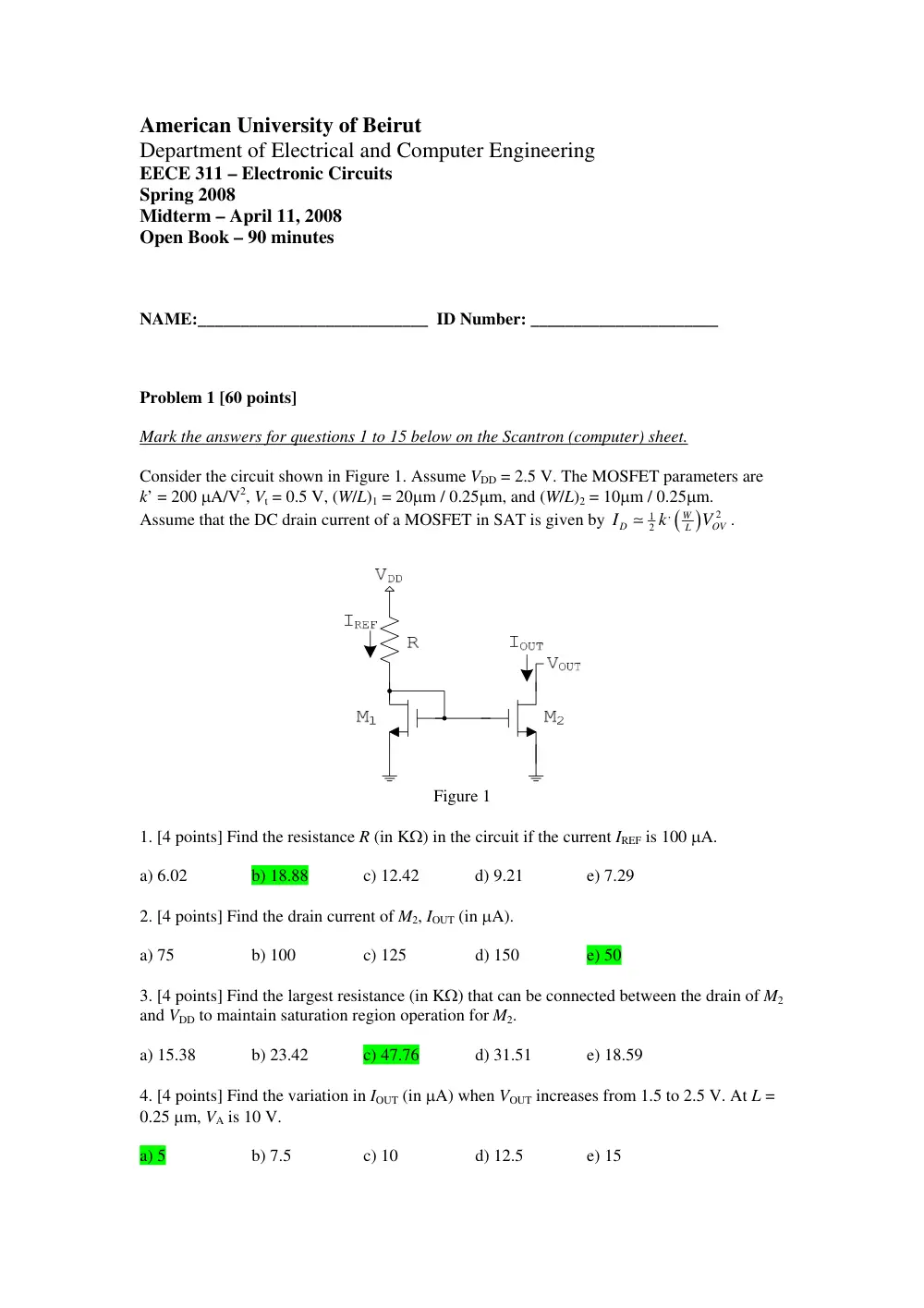
Consider the circuit shown in Figure 1. Assume VDD = 2.5 V. The MOSFET parameters are
k’ = 200 μA/V2, Vt = 0.5 V, (W/L)1 = 20μm / 0.25μm, and (W/L)2 = 10μm / 0.25μm.
Assume that the DC drain current of a MOSFET in SAT is given by
( )
,
2
1
2
W
D
OV
L
I
k
V
�
.
Figure 1
1. [4 points] Find the resistance R (in KΩ) in the circuit if the current IREF is 100 μA.
a) 6.02
b) 18.88
c) 12.42
d) 9.21
e) 7.29
2. [4 points] Find the drain current of M2, IOUT (in μA).
a) 75
b) 100
c) 125
d) 150
e) 50
3. [4 points] Find the largest resistance (in KΩ) that can be connected between the drain of M2
and VDD to maintain saturation region operation for M2.
a) 15.38
b) 23.42
c) 47.76
d) 31.51
e) 18.59
4. [4 points] Find the variation in IOUT (in μA) when VOUT increases from 1.5 to 2.5 V. At L =
0.25 μm, VA is 10 V.
a) 5
b) 7.5
c) 10
d) 12.5
e) 15
5. [4 points] Repeat question 4, assuming that (W/L)2 is changed from 10μm / 0.25μm to
40μm / 1μm.
a) 3.75
b) 1.25
c) 1.88
d) 2.50
e) 3.13
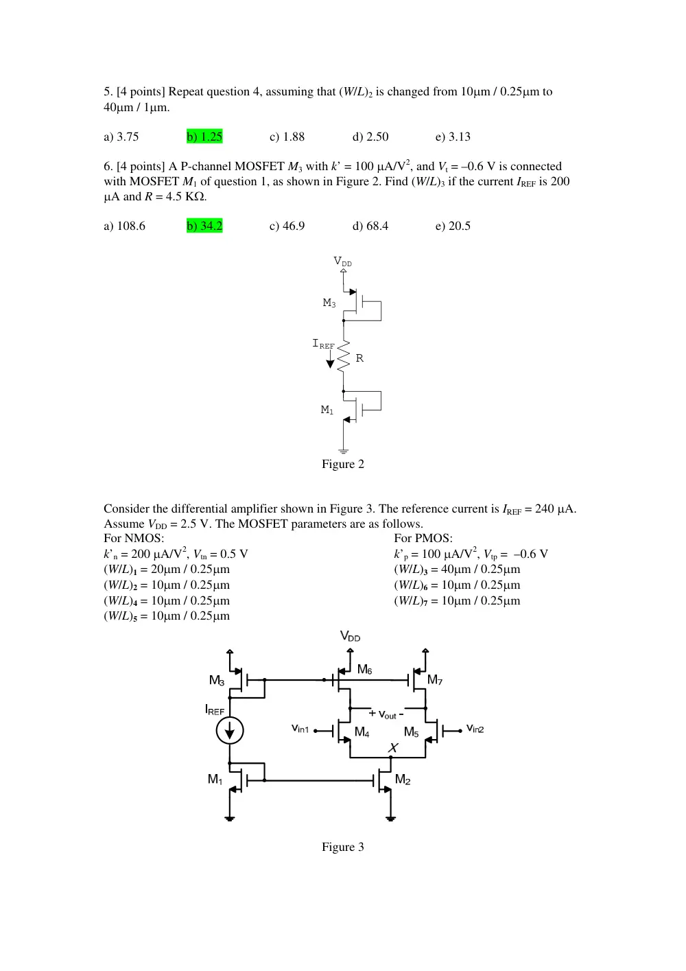
6. [4 points] A P-channel MOSFET M3 with k’ = 100 μA/V2, and Vt = –0.6 V is connected
with MOSFET M1 of question 1, as shown in Figure 2. Find (W/L)3 if the current IREF is 200
μA and R = 4.5 KΩ.
a) 108.6
b) 34.2
c) 46.9
d) 68.4
e) 20.5
IREF
R
M1
VDD
M3
Figure 2
Consider the differential amplifier shown in Figure 3. The reference current is IREF = 240 μA.
Assume VDD = 2.5 V. The MOSFET parameters are as follows.
For NMOS:
For PMOS:
k’n = 200 μA/V2, Vtn = 0.5 V
k’p = 100 μA/V2, Vtp = –0.6 V
(W/L)1 = 20μm / 0.25μm
(W/L)3 = 40μm / 0.25μm
(W/L)2 = 10μm / 0.25μm
(W/L)6 = 10μm / 0.25μm
(W/L)4 = 10μm / 0.25μm
(W/L)7 = 10μm / 0.25μm
(W/L)5 = 10μm / 0.25μm
Figure 3
7. [4 points] Find the DC voltage (in mV) at node X when the two inputs are at 0.9 V.
a) 258.6
b) 250.0
c) 277.5
d) 267.7
e) 288.2
8. [4 points] Find the total power dissipation (in mW) in the circuit.
a) 0.90
b) 1.05
c) 1.20
d) 1.35
e) 0.75
Assume in the following that VAN = 10 V, and |VAP | = 8 V.
9. [4 points] Find the small-signal differential gain vout/(vin1 – vin2).
a) –79.5
b) –72.6
c) –67.2
d) –62.9
e) –59.3
10. [4 points] Find the small-signal differential gain vout/(vin1 – vin2) when a 1000 KΩ resistor
is connected across the vout terminals.
a) –53.9
b) –56.6
c) –67.5
d) –63.2
e) –59.6
11. [4 points] Find the small-signal common-mode gain when the output is taken single-
endedly (at the drain of M4 or M5). In this case, v1 = v2 = vicm.
a) –2.8
b) –0.008
c) –0.08
d) –0.8
e) –1.8
12. [4 points] Find the small-signal common-mode gain when the output is taken
differentially. In this case, v1 = v2 = vicm.
a) 0
b) 0.08
c) –0.08
d) –0.008
e) 0.008
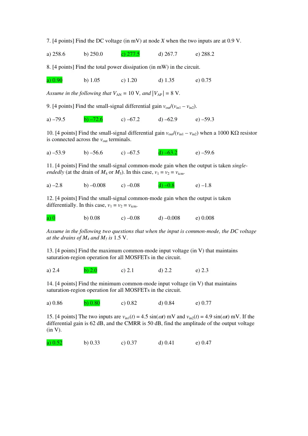
Assume in the following two questions that when the input is common-mode, the DC voltage
at the drains of M4 and M5 is 1.5 V.
13. [4 points] Find the maximum common-mode input voltage (in V) that maintains
saturation-region operation for all MOSFETs in the circuit.
a) 2.4
b) 2.0
c) 2.1
d) 2.2
e) 2.3
14. [4 points] Find the minimum common-mode input voltage (in V) that maintains
saturation-region operation for all MOSFETs in the circuit.
a) 0.86
b) 0.80
c) 0.82
d) 0.84
e) 0.77
15. [4 points] The two inputs are vin1(t) = 4.5 sin(ωt) mV and vin2(t) = 4.9 sin(ωt) mV. If the
differential gain is 62 dB, and the CMRR is 50 dB, find the amplitude of the output voltage
(in V).
a) 0.52
b) 0.33
c) 0.37
d) 0.41
e) 0.47
Problem 2 [40 points]
Solve this problem on the answer booklet.
The common-emitter amplifier shown in Figure 4 is biased using IREF = 140 μA, and has
VAn = 10 V, |VAp| = 5 V, and large β. Q2 and Q3 are matched. In DC analysis, assume that the
collector current in ACTIVE is given by
VBE
VT
C
S
I
� I e
, where VT = 25 mV.
Figure 4
a) [5 points] Find the output resistance of the amplifier. Assume all transistors are an internal
part of the amplifier.
The output resistance is ro(Q1) // ro(Q2)
Since Q2 and Q3 are matched, and β is very large: IC1 = IC2 = IREF = 140 μA.
ro(Q1) = VAN / IC1 = 10/0.14 = 71.43 KΩ
ro(Q2) = |VAP| / IC1 = 5/0.14 = 35.71 KΩ
Rout = ro(Q1) // ro(Q2) = 71.43 // 35.71 = 23.81 KΩ
b) [5 points] Find the open-circuit voltage gain vo/vi.
The open circuit voltage gain vo/vi is –gm1 Rout
gm1 = IC1/VT = 0.14/25 = 5.6 mA/V
vo/vi = –gm1 Rout = –5.6 × 23.81 = –133.34 V/V
Assume in the following that a signal source is connected to the input of the amplifier. It is a
voltage source vsig with a source resistance Rsig = 25 KΩ. Assume also that a 10 KΩ load
resistor is connected from the output to ground. The signal source and the load do not affect
the DC bias.
c) [4 points] Find the input resistance vi/ii of the amplifier if β = 200.
The input resistance vi/ii is rπ = VT/IB = β VT/IC = 200 × 25/0.14 = 35.71 KΩ
d) [4 points] Find the voltage gain vo/vsig.
The voltage gain is –gm1 R’L × (voltage divider ratio at input).
R’L = Rout // RL = 23.81 // 10 = 7.04 KΩ
The voltage divider ratio at the input is rπ / ( rπ + Rsig) = 35.71 / (35.71+25) = 0.5882
The voltage gain vo/vsig = –5.6 × 7.04 × 0.5882 = –23.19 V/V
Assume now that for Q1, Cπ = 25 fF, Cμ = 10 fF, and that a load capacitance CL = 40 fF is
connected from the output to ground. Neglect all other capacitances.
e) [5 points] Using Miller’s theorem, and assuming that the input circuit determines the upper
3-dB frequency fH, find the value of fH.
The Miller constant K is vc/vb = –gm1 R’L = –5.6 × 7.04 = –39.42
We apply Miller’s theorem to obtain the input capacitance:
The input capacitance is Cin = Cπ + (1 – K)Cμ = 25 + (1+39.42) ×10 = 429.2 fF
The resistance seen by this input capacitance is rπ // Rsig = 35.71 // 25 = 14.71 KΩ
The 3-dB frequency due to the input circuit is
fH = 1/(2π Cin (rπ // Rsig)) = 1/(2π × 429.2 f × 14.71 K) = 25.21 MHz
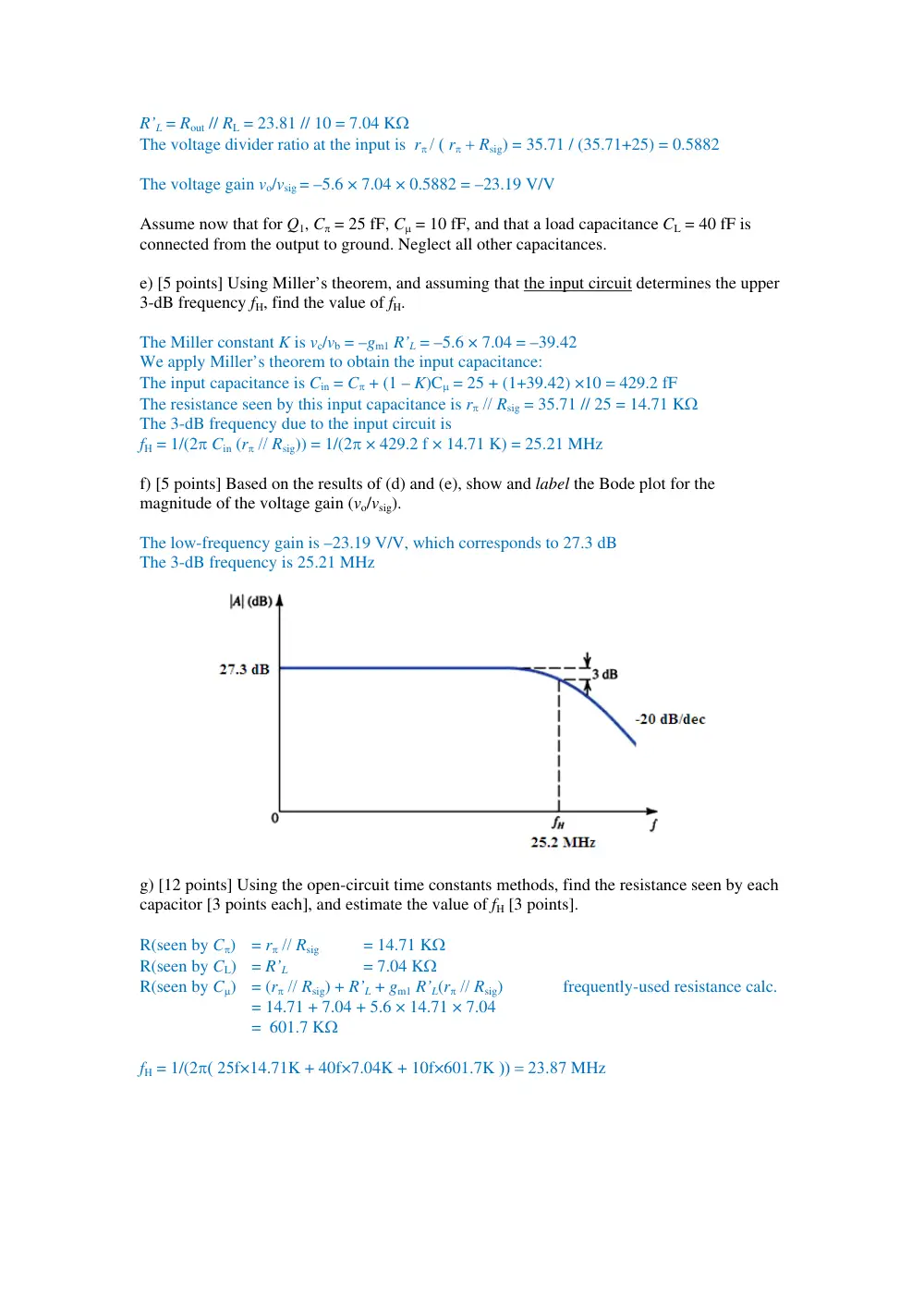
f) [5 points] Based on the results of (d) and (e), show and label the Bode plot for the
magnitude of the voltage gain (vo/vsig).
The low-frequency gain is –23.19 V/V, which corresponds to 27.3 dB
The 3-dB frequency is 25.21 MHz
g) [12 points] Using the open-circuit time constants methods, find the resistance seen by each
capacitor [3 points each], and estimate the value of fH [3 points].
R(seen by Cπ) = rπ // Rsig
= 14.71 KΩ
R(seen by CL) = R’L
= 7.04 KΩ
R(seen by Cμ) = (rπ // Rsig) + R’L + gm1 R’L(rπ // Rsig) frequently-used resistance calc.
= 14.71 + 7.04 + 5.6 × 14.71 × 7.04
= 601.7 KΩ
fH = 1/(2π( 25f×14.71K + 40f×7.04K + 10f×601.7K )) = 23.87 MHz