
EECE 320 Problems Recitations Solutions, Fall 2011
American University of Beirut · Digital Systems Design · 44 pages · Dr. Lama Hamandi · with solution

Showing the first 10 of 44 pages. Download the PDF to see all of it.
More EECE 320 files
- Problems · Fall 2010ProblemsView
- Problems Important Problems on Memory, Flip Flops · Fall 2010ProblemsView
- Homework 2 · Fall 2016HomeworkView
- Homework 4 · Summer 2016HomeworkView
- Homework 2 and 3 · Summer 2016HomeworkView
- Homework 1 · Summer 2016HomeworkView
- Homework 1 · Fall 2016HomeworkView
- Homework 3 · Fall 2016HomeworkView
Show the text of this problems
American University of Beirut
Department of Electrical and Computer Engineering
EECE 320 – Digital Systems Design
Problem session 3
1) Using VHDL, design your previous circuit using
a- behavioral architecture
b- dataflow architecture
Write a corresponding test bench where all input cases are accounted for, and simulate
your result for all previous implementations.
EECE 320
Problem session 3 Solution
Problem 1
Behavioral:
library ieee;
use ieee.std_logic_1164.all;
entity BCD_detector is
port( B8,B4,B2,B1 : in std_logic;
F : out std_logic );
end BCD_detector;
architecture behavioral of BCD_detector is
begin
process(B8,B4,B2)
begin
if B8 = '1' and B4 = '1' then F <= '1';
elsif B8 = '1' and B2 = '1' then F <= '1';
else F <= '0'; end if;
end process;
end behavioral;
Dataflow:
architecture dataflow of BCD_detector is
begin
F <= ((B8 and B4) or (B8 and B2));
end dataflow;
Testbench:
library ieee;
use ieee.std_logic_1164.all;
entity testbench is
end testbench;
architecture testbench of testbench is
component BCD_detector port( B8,B4,B2,B1 : in std_logic; F : out std_logic ); end component;
signal B8 : std_logic :='0';
signal B4 : std_logic :='0';
signal B2 : std_logic :='0';
signal B1 : std_logic :='0';
signal F : std_logic;
begin
BCD : BCD_detector port map (B8, B4, B2, B1,F);
B1 <= Not B1 after 1 ns;
B2 <= Not B2 after 2 ns;
B4 <= Not B4 after 4 ns;
B8 <= Not B8 after 8 ns;
end testbench;
Waveform:
American University of Beirut
Department of Electrical and Computer Engineering
EECE 320 – Digital Systems Design
Problem session 4
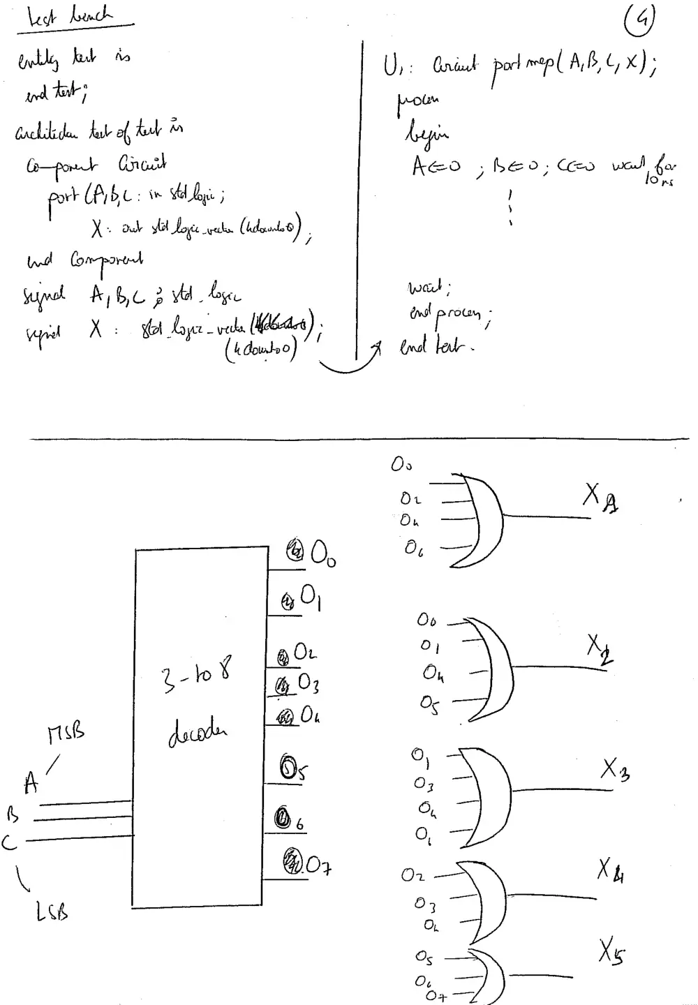
1) Design a 5-to-32 bit decoder with active low enable and active low outputs using as
many 2-to-4 decoders with active low enable as you need as well as one additional
decoder with active low enable having active low outputs that you have to properly
choose. Draw the block diagram of your design.
2) We would like to simulate the circuit that you just designed in problem2 using VHDL.
For that define an entity decoder2to4 and use a dataflow description for it, define an
entity decoderx for that additional decoder that you used and write a behavioral
description for it then define an entity decoder5to32 and write a structural description for
it using the previous two entities. Write also a testbench for your decoder and simulate it
on ModelSim.
EECE 320
Problem Session 4 Solution
Problem 2
Problem 3
2 to 4 decoder
library ieee;
use ieee.std_logic_1164.all;
entity decoder2to4 is
port ( I: in std_logic_vector(1 downto 0);
En : in std_logic;
O: out std_logic_vector(0 to 3));
end decoder2to4;
architecture dataflow of decoder2to4 is
begin
O(0) <= I(0) OR I(1) OR En;
O(1) <= (NOT I(0)) OR I(1) OR En;
O(2) <= I(0) OR (NOT I(1)) OR En;
O(3) <= (NOT I(0)) OR (NOT I(1)) OR En;
LSB
LSB
end dataflow;
3 to 8 decoder
library ieee;
use ieee.std_logic_1164.all;
entity decoder3to8 is
port( I : in std_logic_vector(2 downto 0);
En : in std_logic;
O : out std_logic_vector(0 to 7) );
end decoder3to8;
architecture behavioral of decoder3to8 is
signal Y: std_logic_vector(0 to 7);
begin
process(I,En)
begin
case I is
when "000" => Y <= "01111111";
when "001" => Y <= "10111111";
when "010" => Y <= "11011111";
when "011" => Y <= "11101111";
when "100" => Y <= "11110111";
when "101" => Y <= "11111011";
when "110" => Y <= "11111101";
when "111" => Y <= "11111110";
when others => Y <= "11111111";
end case;
if En = '0' then O <= Y;
else O <= "11111111";
end if;
end process;
end behavioral;
5 to 32 decoder
library ieee;
use ieee.std_logic_1164.all;
entity decoder5to32 is
port( I : in std_logic_vector(4 downto 0);
En : in std_logic;
O : out std_logic_vector(0 to 31) );
end decoder5to32;
architecture structural of decoder5to32 is
component decoder3to8
port ( I : in std_logic_vector(2 downto 0);
En : in std_logic;
O : out std_logic_vector(0 to 7) );
end component;
component decoder2to4
port( I : in std_logic_vector(1 downto 0);
En : in std_logic;
O : out std_logic_vector(0 to 3) );
end component;
signal Y : std_logic_vector(0 to 7);
begin
X : decoder3to8 port map (I => I(4 downto 2), En => En, O => Y);
g : for b in 0 to 7 generate
D: decoder2to4 port map(I => I(1 downto 0),
En => Y(b),
O => O( (4*b) to(4*b+3)));
end generate;
end structural;
Testbench
library ieee;
use ieee.std_logic_1164.all;
entity testbench is
end testbench;
architecture testbench of testbench is
component decoder5to32
port( I : in std_logic_vector(4 downto 0);
En : in std_logic;
O : out std_logic_vector(0 to 31) );
end component;
signal I : std_logic_vector(4 downto 0);
signal En : std_logic := '0';
signal O : std_logic_vector(0 to 31);
begin
Dec : decoder5to32 port map (I, En,O);
process
begin
I <= "00000"; wait for 10 ns;
I <= "00001"; wait for 10 ns;
I <= "00010"; wait for 10 ns;
I <= "00011"; wait for 10 ns;
I <= "00100"; wait for 10 ns;
I <= "00101"; wait for 10 ns;
I <= "00110"; wait for 10 ns;
I <= "00111"; wait for 10 ns;
I <= "01000"; wait for 10 ns;
I <= "01001"; wait for 10 ns;
I <= "01010"; wait for 10 ns;
I <= "01011"; wait for 10 ns;
I <= "01100"; wait for 10 ns;
I <= "01101"; wait for 10 ns;
I <= "01111"; wait for 10 ns;
I <= "10000"; wait for 10 ns;
I <= "10001"; wait for 10 ns;
I <= "10100"; wait for 10 ns;
I <= "11010"; wait for 10 ns;
I <= "11110"; wait for 10 ns;
I <= "11111"; wait for 10 ns;
En <= '1' ; wait for 10 ns;
I <= "00001"; wait for 10 ns;
I <= "01001"; wait for 10 ns;
I <= "10000"; wait for 10 ns;
I <= "11111"; wait for 10 ns;
wait;
end process;
end testbench;
Waveform:
American University of Beirut
Department of Electrical and Computer Engineering
EECE 320 – Digital Systems Design
Problem session 5
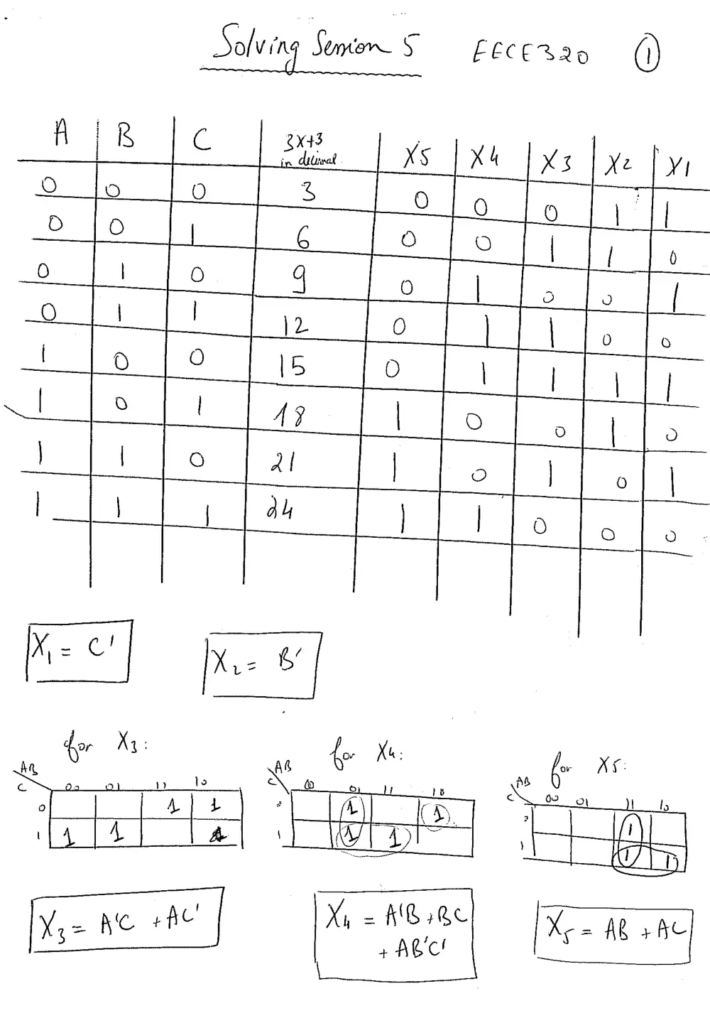
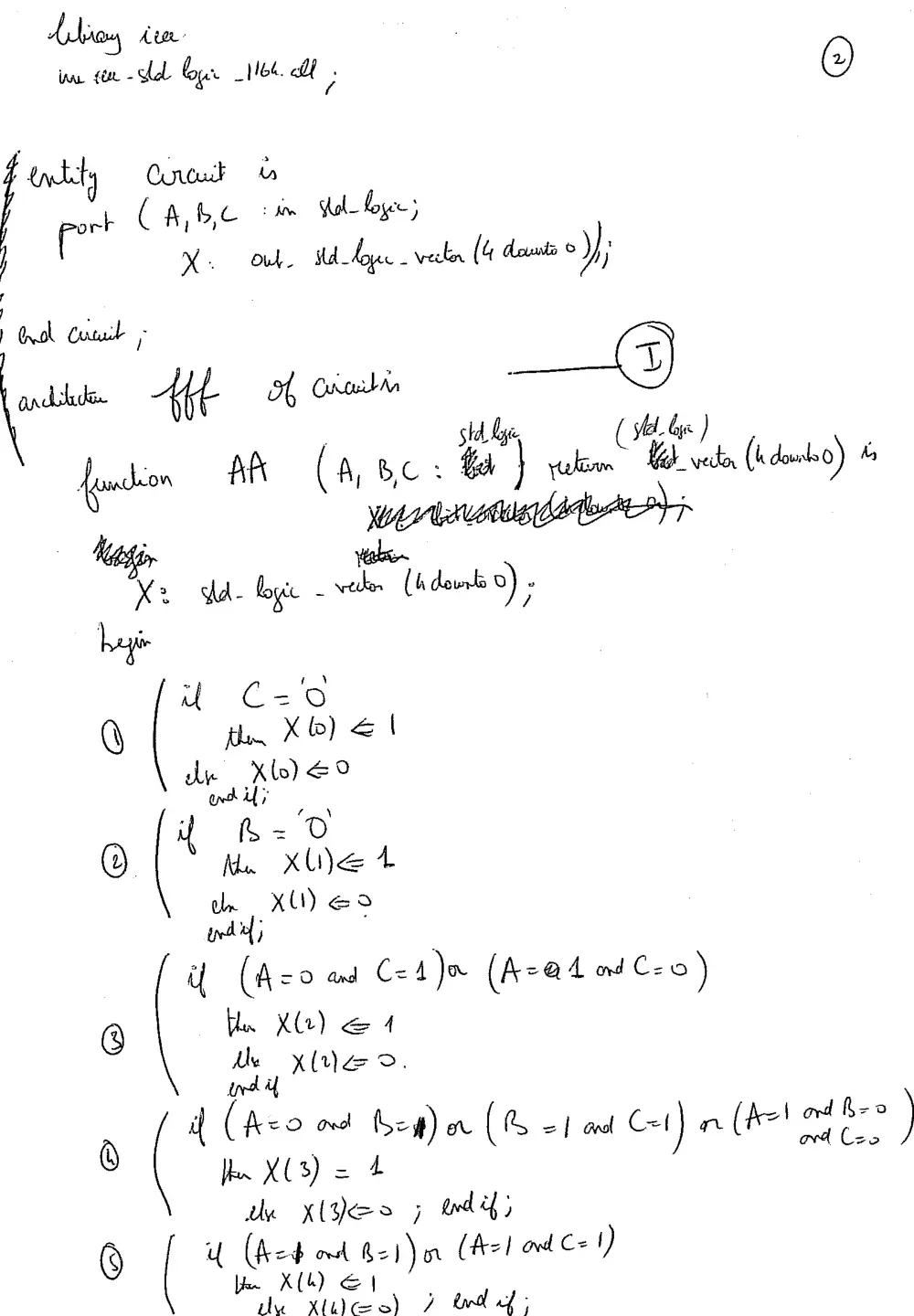
1) Consider problem 1 designed in Assignment 4: Design a combinational circuit that
accepts a 3-bit number and generates an output equal to 3X+3.
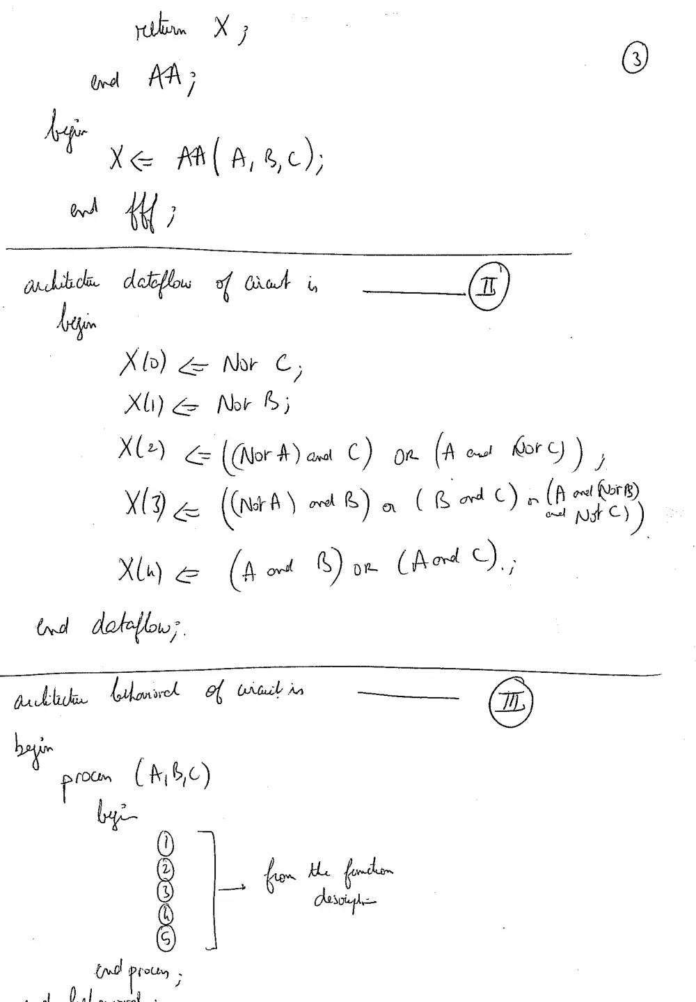
We would like to simulate the previous circuit using VHDL. Write different descriptions
for it.
a- using a function,
b- dataflow description (without a function)
c- behavioral description (without a function)
Write also a testbench.
2) Design the same problem using the proper size decoder and some additional gates.
American University of Beirut
Department of Electrical and Computer Engineering
EECE 320 – Digital Systems Design
Problem Solving Session 2
I - Design a circuit that accepts two 2-bit numbers (A1 A0 , B1 B0 ) and
generate an output equal to the sum of the first and the double of the
second: A1 A0 + 2 * B1 B0.
Solutions:
I -
A
B
C
D
Cout
S1
S0
0
0
0
0
0
0
0
0
0
0
1
0
0
1
0
0
1
0
0
1
0
0
0
1
1
0
1
1
0
1
0
0
0
0
1
0
1
0
1
0
1
0
0
1
1
0
0
1
1
0
1
1
1
1
0
0
1
0
0
0
0
1
0
1
0
0
1
0
1
1
1
0
1
0
1
0
0
1
0
1
1
1
0
1
1
1
0
0
0
1
1
1
1
0
1
1
0
0
1
1
1
0
1
0
1
1
1
1
1
1
1
0
Then draw a Kmap and get a minimal SOP expression for each output.
American University of Beirut
Department of Electrical and Computer Engineering
EECE 320 – Digital Systems Design
Problem Session 6
Dr. Lama Hamandi
Problem 1:
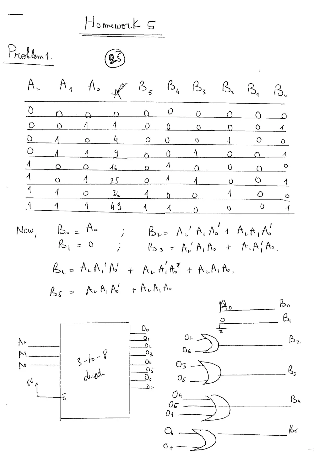
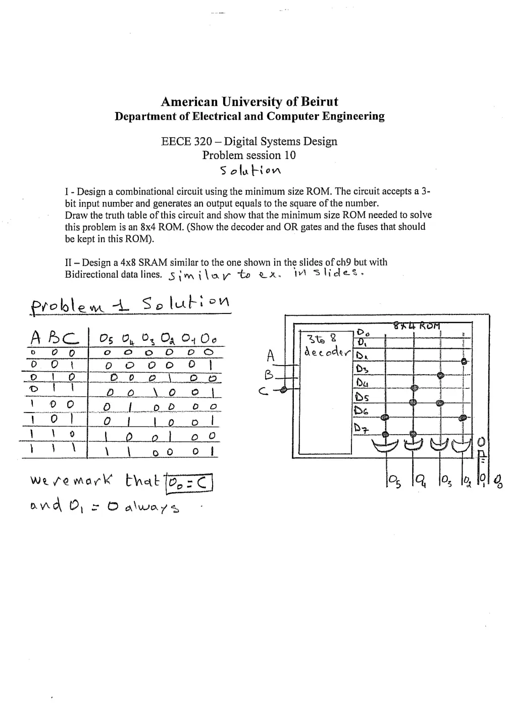
We would like to design a circuit that accepts a 3-bit number and generates its square
using a 3-to-8 decoder with active high output and active high enable and four additional
gates.
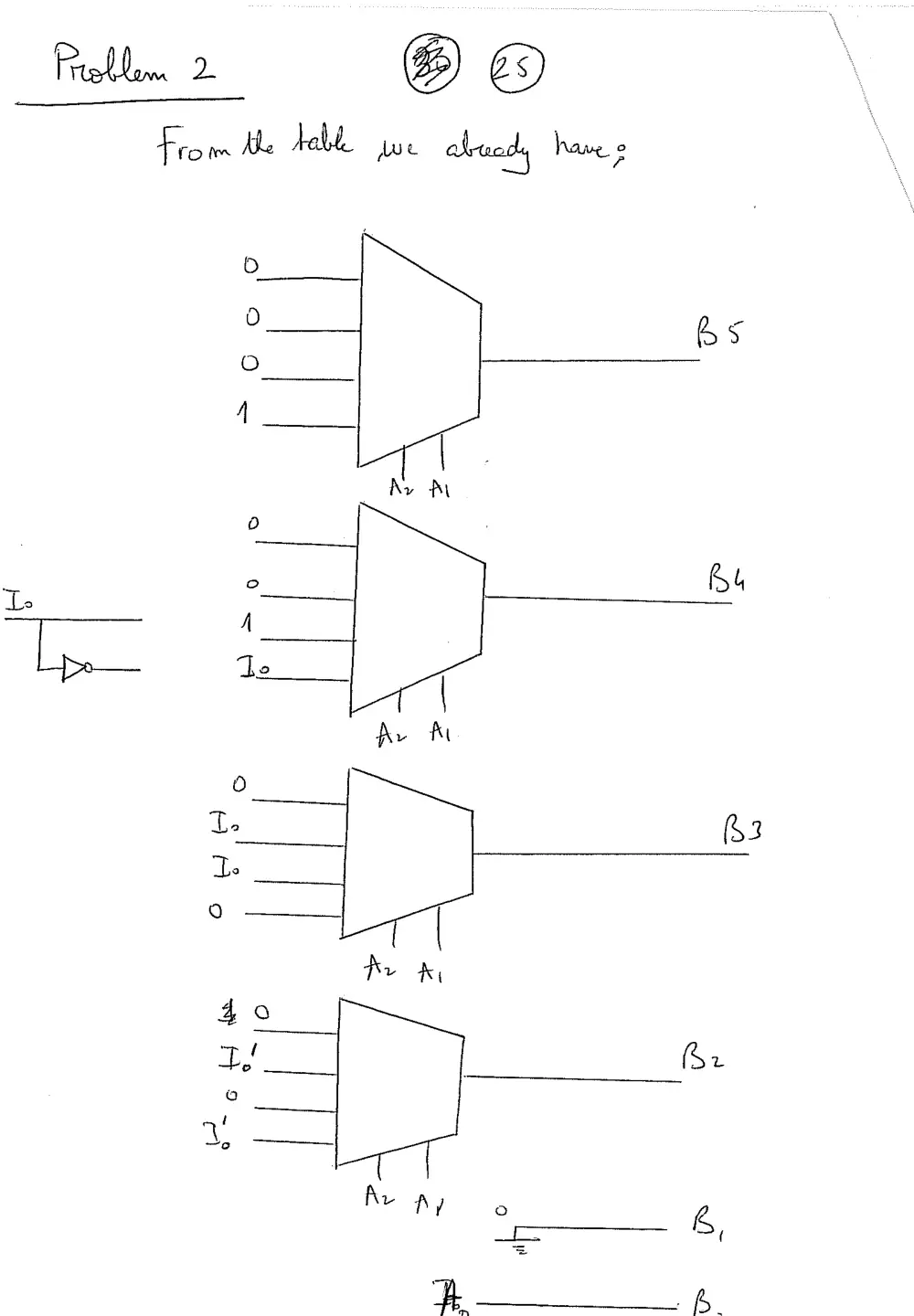
Problem 2:
Repeat problem 1, but use now four 4 to 1 MUXs and an inverter to design this circuit.
Problem 3:
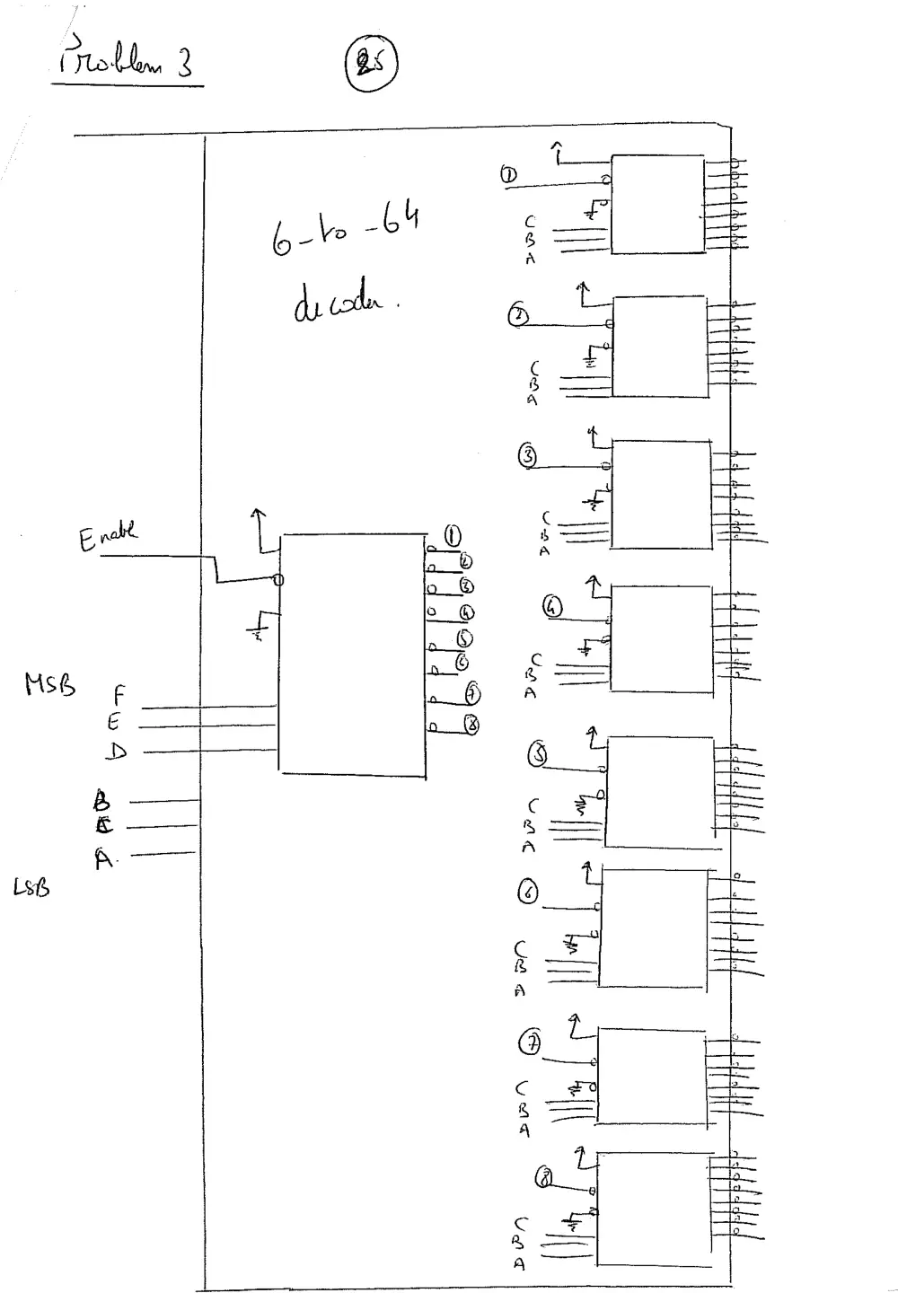
Design a 6-to-64 bit decoder with active low enable and active low outputs using as many
74x138 decoders as you need. Draw the block diagram of your design similar to figure 6-
42 showing the relationship between the modules and properly label all inputs showing
their active levels.
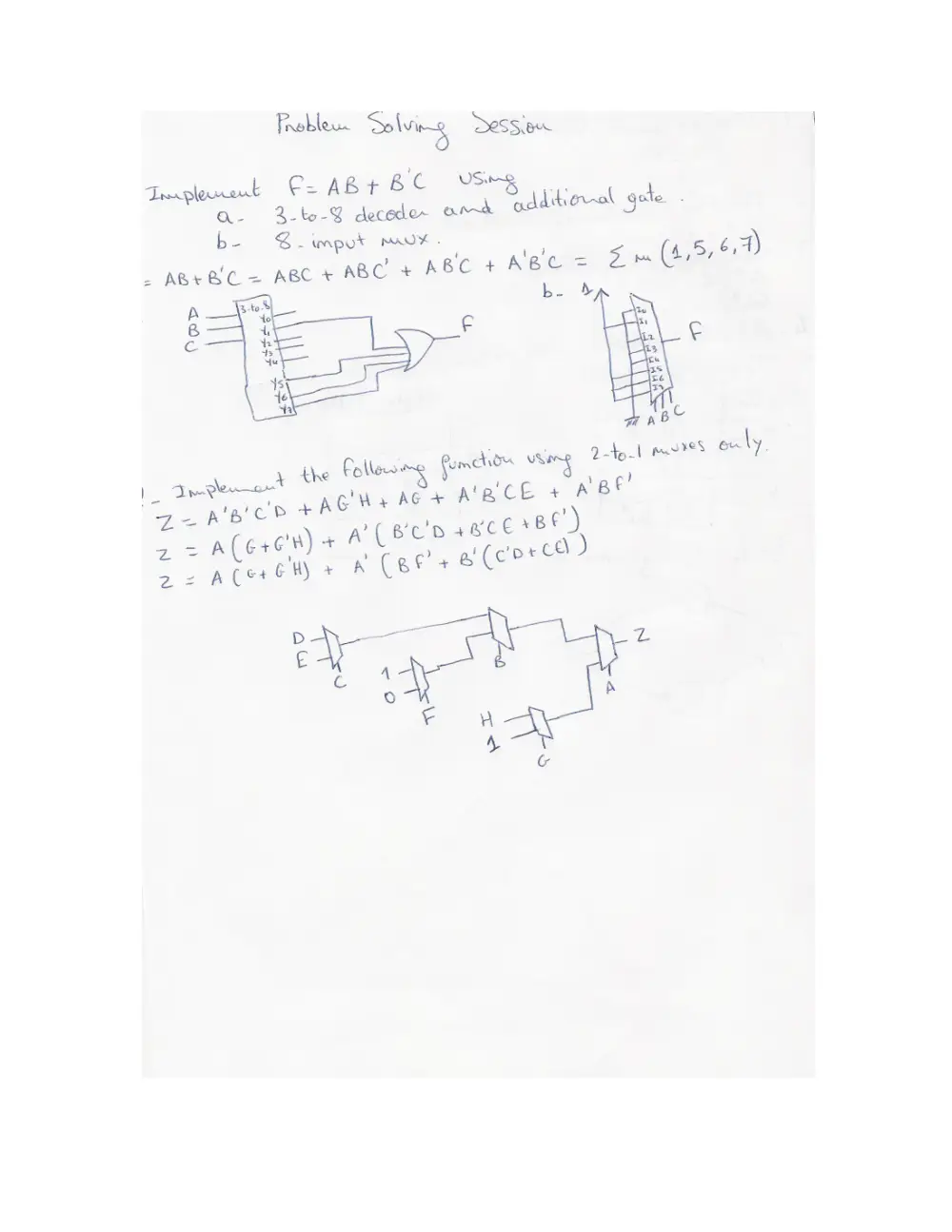
Problem 4:
Problem 5:
American University of Beirut
Department of Electrical and Computer Engineering
EECE 320 – Digital Systems Design
Problem Session 7
Problem 1:
Analyze the following sequential circuit drawing its state/output table and state diagram.
Problem 2: Same question for this circuit:
Z
Problem 1 Solution:
American University of Beirut
Department of Electrical and Computer Engineering
EECE 320 – Digital Systems Design
Problem Session 8
Dr. Lama Hamandi
Problem 1:
Design a sequence detector circuit that has one input X and one output Y. Y=1 if the
input X takes the following sequence of values: 10101. A moore design is required. Use
D FFs.
Complete the timing diagram for this circuit showing how all the state variables change.
Problem 2: A sequential circuit has the following state diagram. Design the circuit using
JK flip flops. Use a minimal cost design.
Problem 3:
Implement in VHDL the previous state diagram.
x=1/
y=0
x=1/
y=1
S1
S2
x=1/
y=0
x=0/
y=1
x=0/
y=0
x=0/
y=0
S0
CLK
X
Problem 1 solution
Problem 2 solution:
American University of Beirut
Department of Electrical and Computer Engineering
EECE 320 – Digital Systems Design
Problem Session 9
Dr. Lama Hamandi
Problem 1:
Draw the circuit implementation of the 8-bit PIPO general shift-register presented in
chapter8 using D FFs and multiplexers.
Problem 2:
Draw the circuit implementation of the 74163 counter defined chapter8 using JK FFs, OR
gates and AND gates.
Problem 3:
Draw the state diagram of the following counter. Show all states.
Solution:
Problem 1:
Problem 2: