
EECE 310 Homework 6 with Solution, Fall 2007
American University of Beirut · Electronics · 7 pages · with solution

More EECE 310 files
- Homework Spice3 Solution · Summer 2012Homework · with solutionView
- Homework Spice2 Solution · Summer 2012Homework · with solutionView
- Homework Spice1 Solution · Summer 2012Homework · with solutionView
- Homework 1 Solution · Fall 2011Homework · with solutionView
- Homework 2 · Fall 2011HomeworkView
- Homework 1 · Fall 2011HomeworkView
- Homework 1 · Fall 2011HomeworkView
- Homework 1 Solution · Fall 2011Homework · with solutionView
Show the text of this homework
American University of Beirut
Department of Electrical and Computer Engineering
EECE 310 – Electronics
Fall 2007 – 2008
Homework 6
Problem 1.
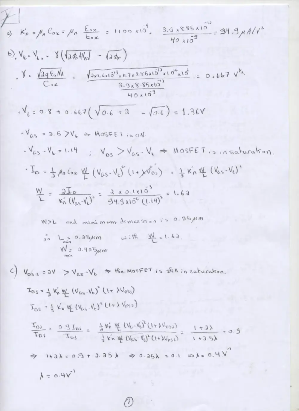
a) The mobility of electrons in the channel of an NMOS device is 1100 cm2/V.sec. Find
the transconductance parameter k’n for this MOSFET if its oxide thickness is 40 nm.
The doping level in the channel is NA = 1016 cm-3. The relative permittivity of the
oxide (SiO2) is 3.9, and that of Silicon is 11.7.
b) The threshold voltage Vt0 for this NMOS transistor is 0.8 V. Find the required
dimensions of the gate of the NMOS transistor (W and L) to get a drain current of
0.1 mA when the MOSFET is biased at (VGS = 2.5 V, VDS = 2.5 V, VBS = 2 V). The
minimum dimension is 0.25 μm.
c) The drain current of the NMOS transistor is ID1 at (VGS = 2.5 V, VDS = 2.5 V). When
VDS becomes 2 V, the current decreases by 10% to 0.9 ID1. Find the channel length
modulation parameter λ of this transistor.
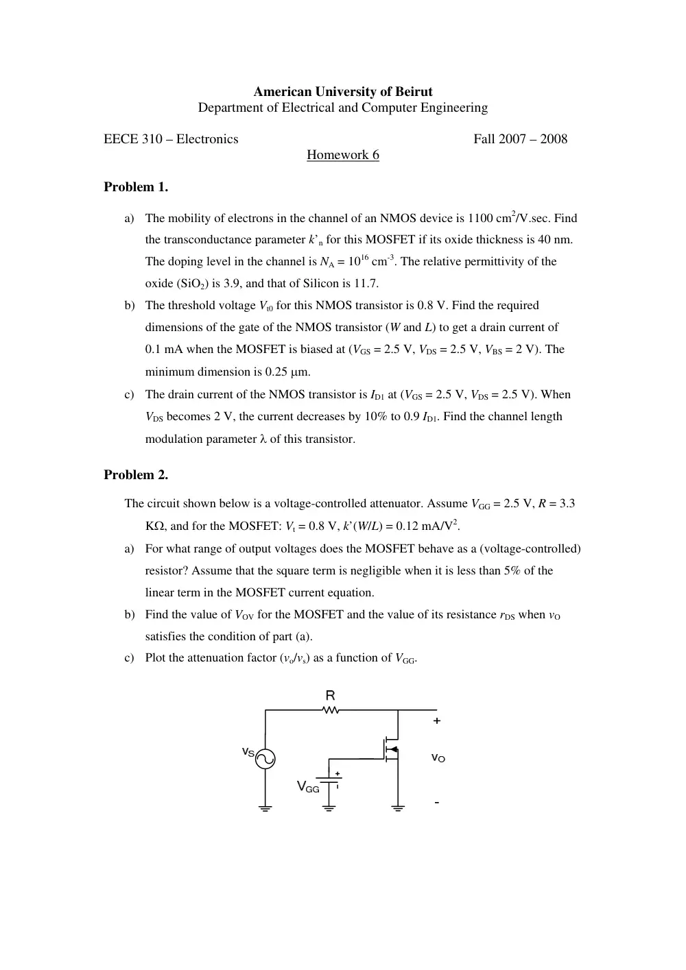
Problem 2.
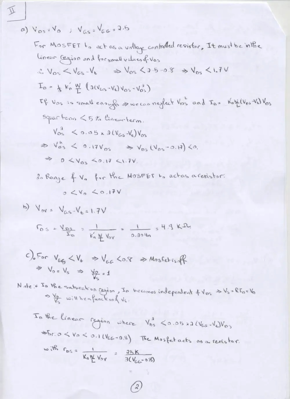
The circuit shown below is a voltage-controlled attenuator. Assume VGG = 2.5 V, R = 3.3
KΩ, and for the MOSFET: Vt = 0.8 V, k’(W/L) = 0.12 mA/V2.
a) For what range of output voltages does the MOSFET behave as a (voltage-controlled)
resistor? Assume that the square term is negligible when it is less than 5% of the
linear term in the MOSFET current equation.
b) Find the value of VOV for the MOSFET and the value of its resistance rDS when vO
satisfies the condition of part (a).
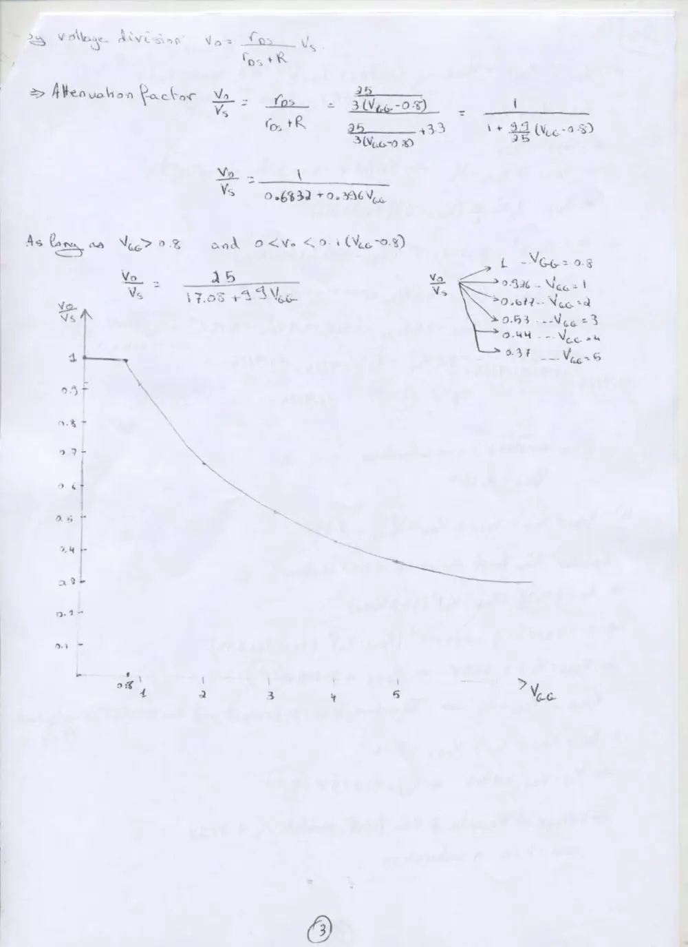
c) Plot the attenuation factor (vo/vs) as a function of VGG.
Problem 3.
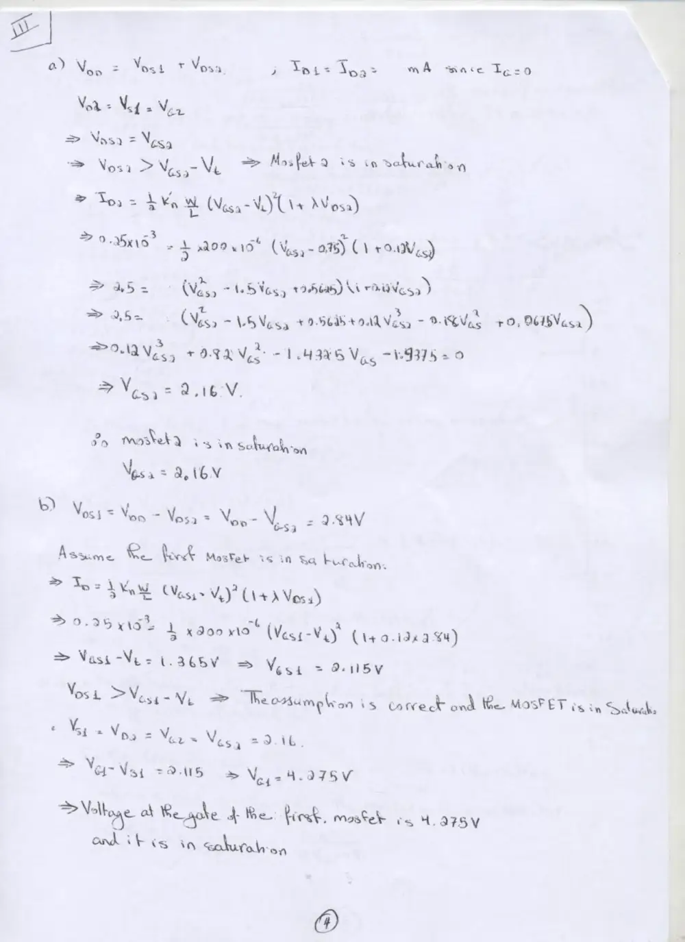
Two identical enhancement MOSFETs with k’n(W/L) = 200 μA/V2, Vt = 0.75 V, and λ =
0.12 V-1 are connected as shown below. The MOSFET drain current is 0.25 mA.
Assume that VDD = 5 V.
a) Find the value of VGS for the lower MOSFET. In what region is this MOSFET
operating?
b) Find the voltage at the gate of the upper MOSFET. In what region is this MOSFET
operating?
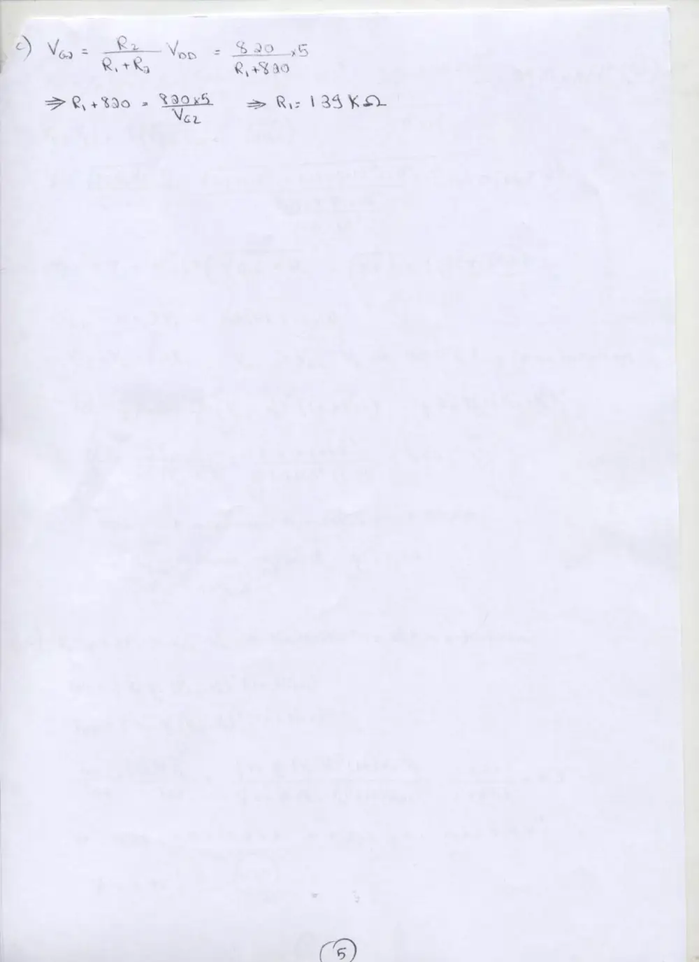
c) Find the resistance R1 when R2 = 820 KΩ.