
EECE 310 Homework 8 with Solution, Fall 2007
American University of Beirut · Electronics · 10 pages · with solution


More EECE 310 files
- Homework Spice3 Solution · Summer 2012Homework · with solutionView
- Homework Spice2 Solution · Summer 2012Homework · with solutionView
- Homework Spice1 Solution · Summer 2012Homework · with solutionView
- Homework 1 Solution · Fall 2011Homework · with solutionView
- Homework 2 · Fall 2011HomeworkView
- Homework 1 · Fall 2011HomeworkView
- Homework 1 · Fall 2011HomeworkView
- Homework 1 Solution · Fall 2011Homework · with solutionView
Show the text of this homework
American University of Beirut
Department of Electrical and Computer Engineering
EECE 310 – Electronics
Fall 2007 – 2008
Homework 8
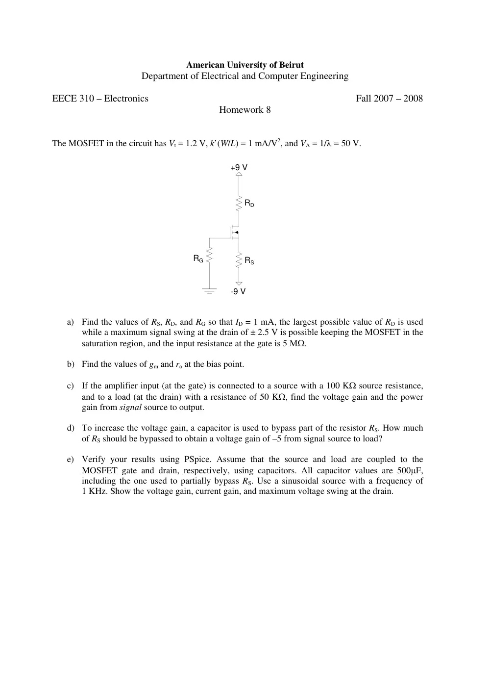
The MOSFET in the circuit has Vt = 1.2 V, k’(W/L) = 1 mA/V2, and VA = 1/λ = 50 V.
RG
+9 V
RD
RS
-9 V
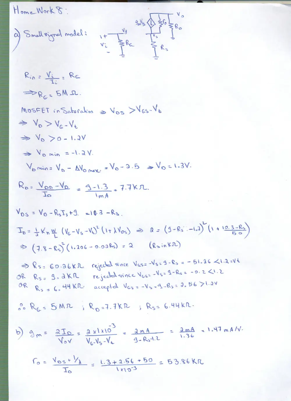
a) Find the values of RS, RD, and RG so that ID = 1 mA, the largest possible value of RD is used
while a maximum signal swing at the drain of ± 2.5 V is possible keeping the MOSFET in the
saturation region, and the input resistance at the gate is 5 MΩ.
b) Find the values of gm and ro at the bias point.
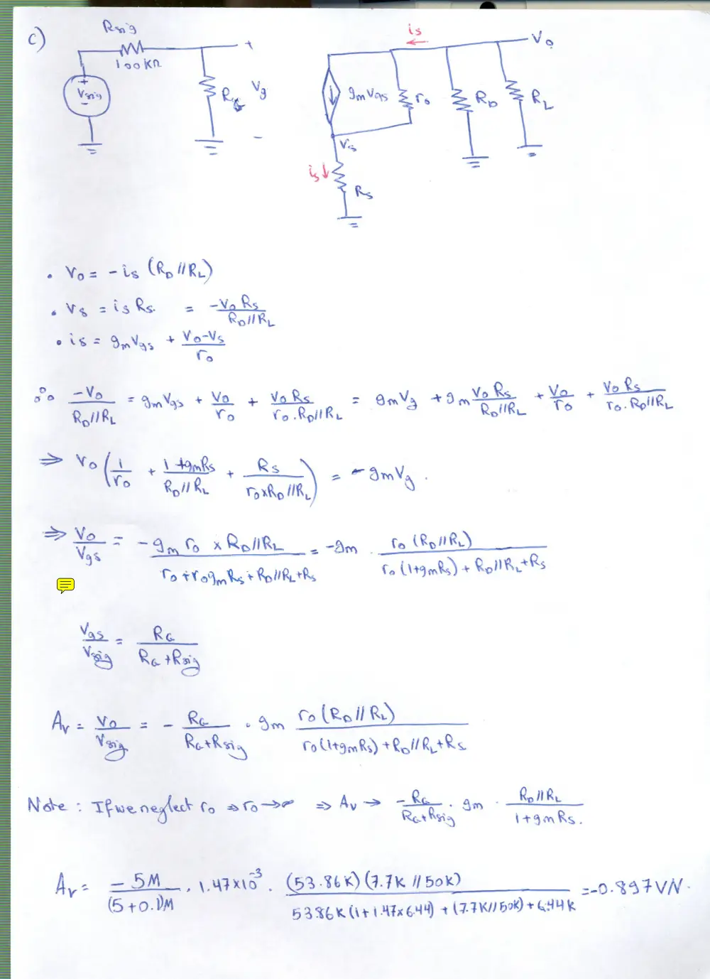
c) If the amplifier input (at the gate) is connected to a source with a 100 KΩ source resistance,
and to a load (at the drain) with a resistance of 50 KΩ, find the voltage gain and the power
gain from signal source to output.
d) To increase the voltage gain, a capacitor is used to bypass part of the resistor RS. How much
of RS should be bypassed to obtain a voltage gain of –5 from signal source to load?
e) Verify your results using PSpice. Assume that the source and load are coupled to the
MOSFET gate and drain, respectively, using capacitors. All capacitor values are 500μF,
including the one used to partially bypass RS. Use a sinusoidal source with a frequency of
1 KHz. Show the voltage gain, current gain, and maximum voltage swing at the drain.
e) For unbypassed Rs
M1
menhn
W = 100um
L = 10um
-1.000mA
0A
1.000mA
C2
500uF
V
0V
0V
RS
6.44k
RL
50k
0A
Vo: red, Vi in green.
Av=Vo/Vi= ‐0.897.248/1= ‐0.897.248
out
Rg
5000K
0A
Rd
7.7k
0V
0V
V
in
C1
500uF
Vs
FREQ = 1KHz
VAMPL = 1mV
VOFF = 0
0A
V1
9Vdc
9.000V
1.000mA
V2
9Vdc
1.303V
1.000mA
R7
100K
Time
5.0ms
5.5ms
6.0ms
6.5ms
7.0ms
7.5ms
8.0ms
V(IN)
V(OUT)
-1.0mV
-0.5mV
0V
0.5mV
1.0mV
(5.7487m,897.248u)
Io in red and Ii in green
Time
5.0ms
5.5ms
6.0ms
6.5ms
7.0ms
7.5ms
8.0ms
-I(Rg)
-I(RL)
-20nA
-10nA
0A
10nA
20nA
(5.7450m,17.945n)
(5.7450m,-195.983p)
Ai=Io/Ii = ‐17.945n/195.983p =91.564 A/A
1 pt
Po in red and Pi in green
Time
5.0ms
5.5ms
6.0ms
6.5ms
7.0ms
7.5ms
8.0ms
W(Rg)
W(RL)
0W
5pW
10pW
15pW
20pW
(5.2450m,16.101p)
(5.2450m,192.045f)
Ap=Po/Pi = 16.1p/192f =83.85 W/W
To find the maximum swing at the drain we can change Vs until VD=VG‐ Vt
Note: The maximum swing here is less than ±2.5V since when we designed the circuit and
calculated the value of RD, we neglected the swing at the gate (swing at drain /Gain).
VD‐2.5 > VG + (2.5/Av) ‐ Vt
However Av turned out to be less than 1 and the swing of 2.5 requires Vg to change by more
than 2.5V which can no longer be neglected. That is why the maximum swing at the drain
here is less than 2.5V.
Trace of VG‐ Vt and VD
Time
5.0ms
5.5ms
6.0ms
6.5ms
7.0ms
7.5ms
8.0ms
V(M1:d)
V(M1:g)-1.2
-4.0V
-2.0V
0V
2.0V
4.0V
(6.2498m,134.531m)
(5.7498m,2.4677)
We find that for Vs=1.3V (amplitude) VD starts to become equal to VG‐ Vt for some values. So
for larger values of Vs we will have distortion. So the maximum swing will be ±1.17V
e) For bypassed Rs
Vo: red, Vi in green.
Av=Vo/Vi= ‐4.993/1= ‐4.993 V/V
V2
9Vdc
out
RL
50k
0A
1.303V
V1
9Vdc
1.000mA
M1
menhn
W = 100um
L = 10um
-1.000mA
0A
1.000mA
Vs2
FREQ = 1KHz
VAMPL = 1mV
VOFF = 0
0A
9.000V
R7
100K
0A
C1
500uF
0V
V
Rd
7.7k
Rsb
5.903k
in
0V
-3.099V
0V
C2
500uF
0V
V
C3
500uF
RS
537
Rg
5000K
0A
Time
5.0ms
5.5ms
6.0ms
6.5ms
7.0ms
7.5ms
8.0ms
V(IN)
V(OUT)
-5.0mV
0V
5.0mV
(5.7450m,4.9938m)
Io in red and Ii in green
Time
5.0ms
5.5ms
6.0ms
6.5ms
7.0ms
7.5ms
8.0ms
1
-I(RL)
2
I(Vs2)
-100nA
-50nA
0A
50nA
100nA
1
-1.0nA
-0.5nA
0A
0.5nA
1.0nA
2
>>
(5.7450m,195.983p)
(5.7450m,99.877n)
Ai=Io/Ii = 99.877n/195.983p =510 A/A
Po in red and Pi in green
Time
5.0ms
5.5ms
6.0ms
6.5ms
7.0ms
7.5ms
8.0ms
1
W(Rg)
2
W(RL)
0W
50fW
100fW
150fW
1 200fW
0W
200pW
400pW
2 600pW
>>
(5.2450m,498.394p)
(5.2472m,192.045f)
Ap=Po/Pi = 498.4p/192f =2595 W/W
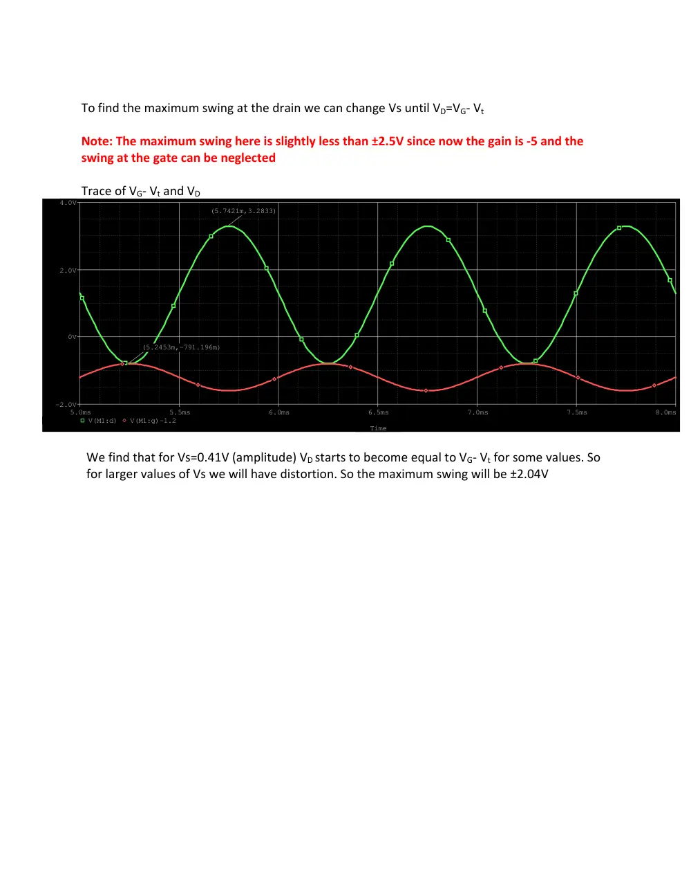
To find the maximum swing at the drain we can change Vs until VD=VG‐ Vt
Note: The maximum swing here is slightly less than ±2.5V since now the gain is ‐5 and the
swing at the gate can be neglected
Trace of VG‐ Vt and VD
Time
5.0ms
5.5ms
6.0ms
6.5ms
7.0ms
7.5ms
8.0ms
V(M1:d)
V(M1:g)-1.2
-2.0V
0V
2.0V
4.0V
(5.2453m,-791.196m)
(5.7421m,3.2833)
We find that for Vs=0.41V (amplitude) VD starts to become equal to VG‐ Vt for some values. So
for larger values of Vs we will have distortion. So the maximum swing will be ±2.04V