
EECE 320 Project 2 Divider, Fall 2010
American University of Beirut · Digital Systems Design · 9 pages · Prof. Ali Chehab


More EECE 320 files
Show the text of this project
EECE 320 – Digital Systems Design
Project 2
Guidelines
You are required to work with the same group as in Project 1.
Any copying will result in serious consequences to all involved students.
8-bit Sequential Divider in VHDL
The aim of this project is to design and test using VHDL a sequential circuit for a 8-bit
divider. The divider should be designed using sequential elements and controlled using a
finite state machine. The 8-bit data inputs to your circuit should be: Dividend A and
Divisor B. The 8-bit data outputs of your circuit should be: Quotient Q and Remainder R.
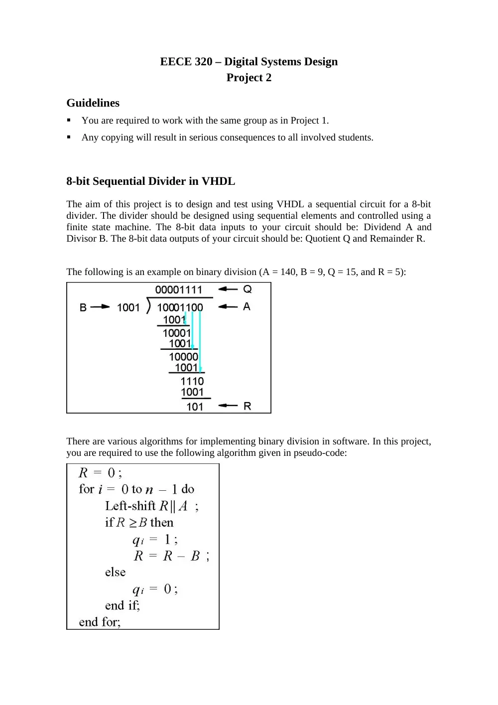
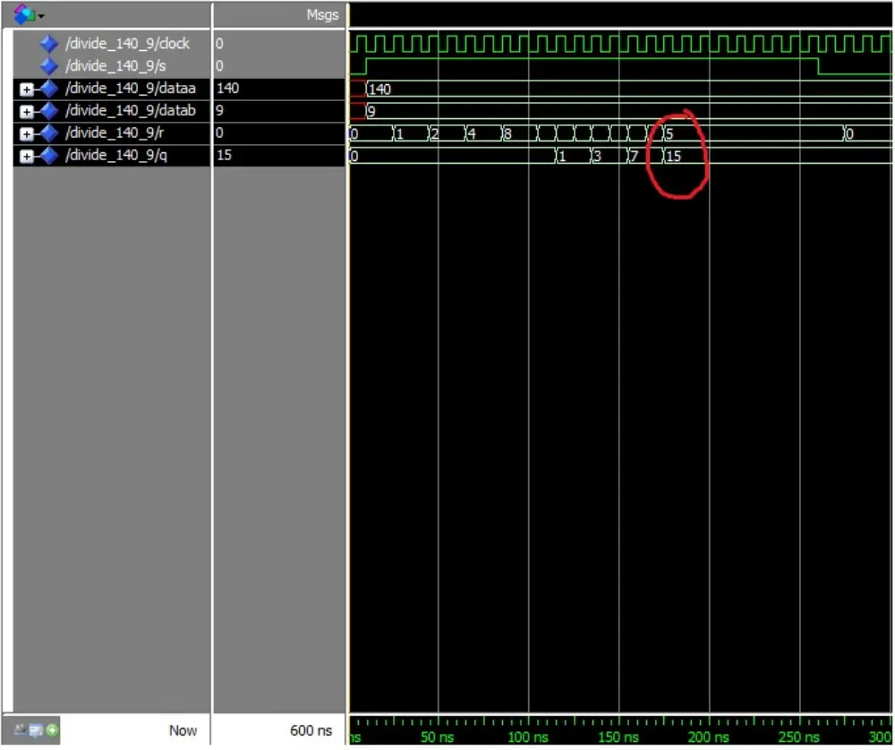
The following is an example on binary division (A = 140, B = 9, Q = 15, and R = 5):
There are various algorithms for implementing binary division in software. In this project,
you are required to use the following algorithm given in pseudo-code:
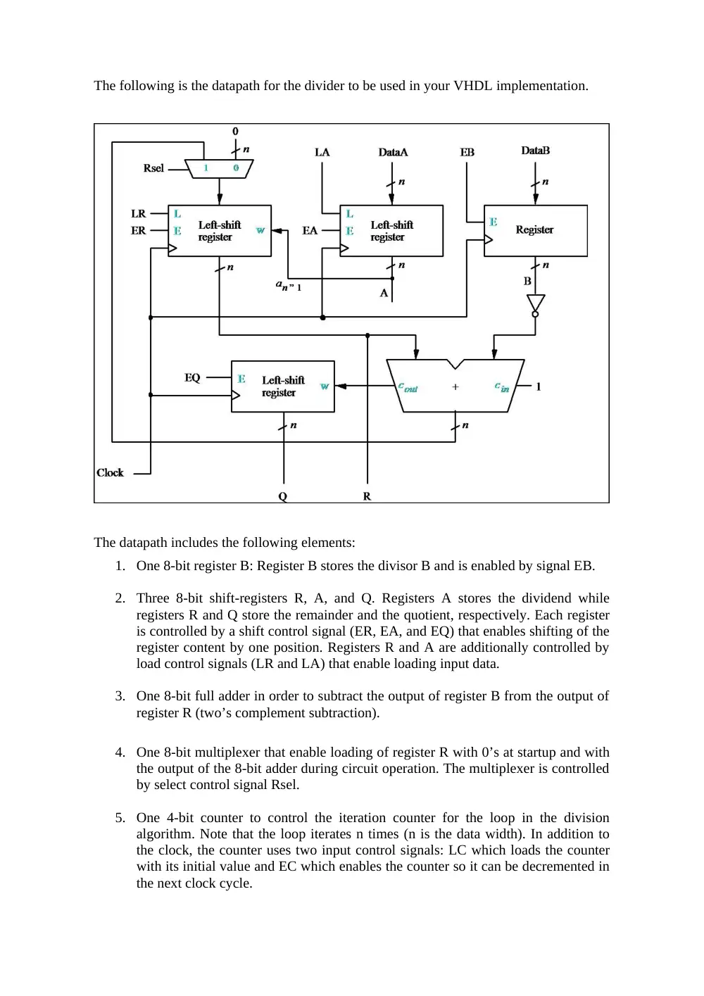
The following is the datapath for the divider to be used in your VHDL implementation.
The datapath includes the following elements:
1. One 8-bit register B: Register B stores the divisor B and is enabled by signal EB.
2. Three 8-bit shift-registers R, A, and Q. Registers A stores the dividend while
registers R and Q store the remainder and the quotient, respectively. Each register
is controlled by a shift control signal (ER, EA, and EQ) that enables shifting of the
register content by one position. Registers R and A are additionally controlled by
load control signals (LR and LA) that enable loading input data.
3. One 8-bit full adder in order to subtract the output of register B from the output of
register R (two’s complement subtraction).
4. One 8-bit multiplexer that enable loading of register R with 0’s at startup and with
the output of the 8-bit adder during circuit operation. The multiplexer is controlled
by select control signal Rsel.
5. One 4-bit counter to control the iteration counter for the loop in the division
algorithm. Note that the loop iterates n times (n is the data width). In addition to
the clock, the counter uses two input control signals: LC which loads the counter
with its initial value and EC which enables the counter so it can be decremented in
the next clock cycle.
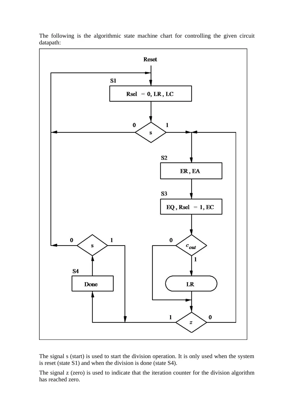
The following is the algorithmic state machine chart for controlling the given circuit
datapath:
The signal s (start) is used to start the division operation. It is only used when the system
is reset (state S1) and when the division is done (state S4).
The signal z (zero) is used to indicate that the iteration counter for the division algorithm
has reached zero.
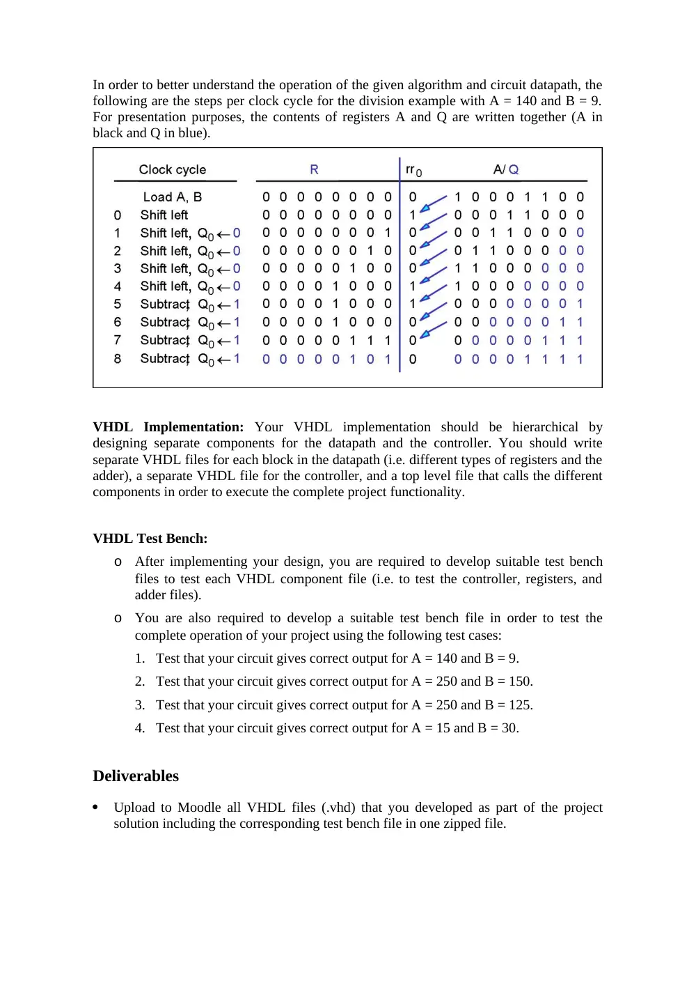
In order to better understand the operation of the given algorithm and circuit datapath, the
following are the steps per clock cycle for the division example with A = 140 and B = 9.
For presentation purposes, the contents of registers A and Q are written together (A in
black and Q in blue).
VHDL Implementation: Your VHDL implementation should be hierarchical by
designing separate components for the datapath and the controller. You should write
separate VHDL files for each block in the datapath (i.e. different types of registers and the
adder), a separate VHDL file for the controller, and a top level file that calls the different
components in order to execute the complete project functionality.
VHDL Test Bench:
o
After implementing your design, you are required to develop suitable test bench
files to test each VHDL component file (i.e. to test the controller, registers, and
adder files).
o
You are also required to develop a suitable test bench file in order to test the
complete operation of your project using the following test cases:
1. Test that your circuit gives correct output for A = 140 and B = 9.
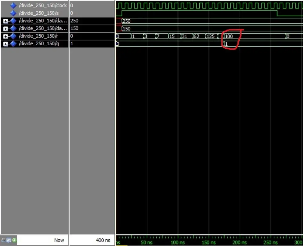
2. Test that your circuit gives correct output for A = 250 and B = 150.
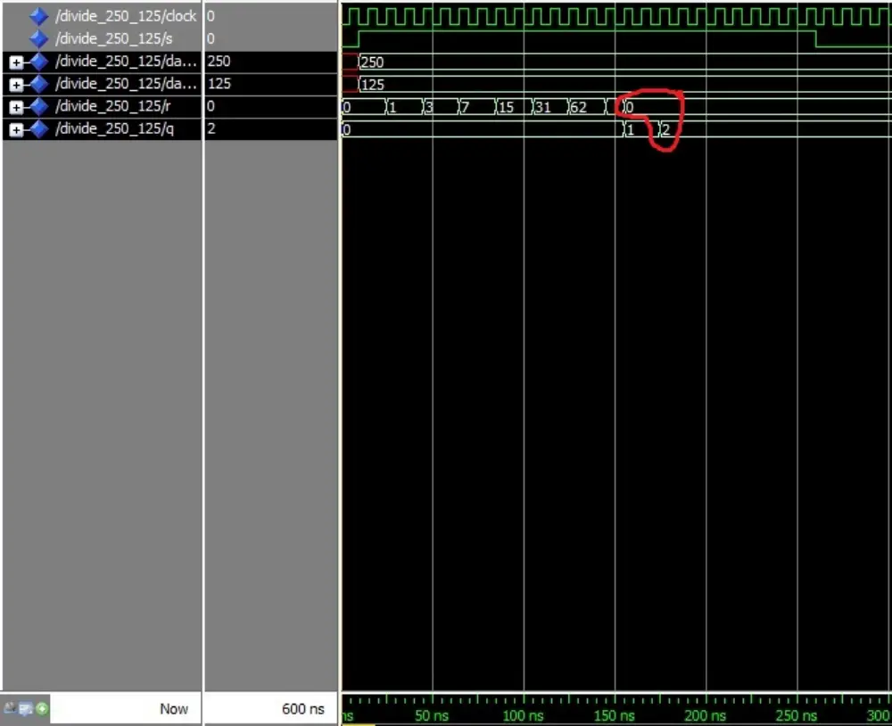
3. Test that your circuit gives correct output for A = 250 and B = 125.
4. Test that your circuit gives correct output for A = 15 and B = 30.
Deliverables
Upload to Moodle all VHDL files (.vhd) that you developed as part of the project
solution including the corresponding test bench file in one zipped file.