
EECE 473 Midterm, Spring 2009
American University of Beirut · Power Electronics · 2 pages · Prof. Sami Karaki

More EECE 473 files
Show the text of this exam
1/6
S. KARAKI
AMERICAN UNIVERSITY OF BEIRUT
FACULTY OF ENGINEERING AND ARCHITECTURE
MIDTERM EXAM
CLOSED BOOK (120 MIN)
POWER ELECTRONICS
APRIL 15, 2009
(EECE 473E)
NAME: ____________________
ID#: ____________________
1. Answer briefly the following questions.
a) What are the gating characteristics of bipolar junction transistors, MOSFETS, and gate turn-off
switches? How many stages there are in a drive circuit and what is a frequently encountered
problem and how is it solved?
b) Discuss how power electronics are used in elevators, electric cars, and HVDC transmission. What
are the main systems or blocks, the devices used, and the control objective in these three
applications and how this objective is achieved?
2. A high-power application magnet is supplied via a three-phase bridge converter from a 1200 V, 50Hz
source. The magnet winding has a resistance R= 2Ω and an inductance L= 200 mH. The three-phase
supply is via a transformer having a per-phase leakage inductance LS= 0.2mH.
a) Draw and label the converter circuit diagram, plot the line-to-neutral supply voltages, the voltage
across the load, the thyristor currents, and the current supplied by the ac source, showing clearly the
effect of commutation overlap. Provide the plots on the attached plot sheets.
b) When the average output voltage value is 1400V calculate the average load current (Io), the firing
angle delay (α), and the angle of commutation overlap (u).
c) Calculate the rms value of the input current, and the rms diode current, the power factor, and the
total harmonic distortion of the input current. Explain briefly formulae used and justify any
approximations.
d) How can the energy stored in the inductor be be recovered by the supply? What is the firing delay
and output voltage needed to recover this energy in minimum time? Bonus: estimate the time
needed!
3. It is required to design a buck converter to supply a permanent dc motor from a 240V dc source. The
motor voltage is to be controlled in the range 100 to 200 V with an allowable peak to peak ripple of 5%.
The motor current is constant at 5A with negligible ripple. The converter may be built using a power
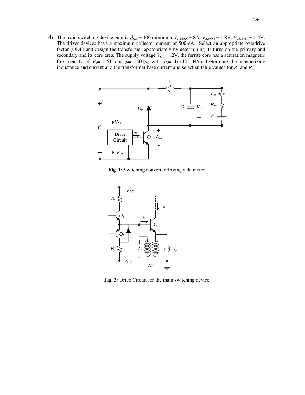
BJT that can operate in the range 1 to 25 kHz. The circuit diagram of the converter is shown in Fig. 1.
a) Describe the operation of the converter clearly identifying which devices are on and off and
describing qualitatively the current and voltage in the various components. Draw the current
waveforms in the inductor, transistor and capacitor, and draw the voltage waveforms across the
capacitor, inductor and diode.
b) Determine the range of duty cycle operation. And given that the frequency is 10 kHz select a proper
value for the inductor L and capacitor C. Note that the current ripple in the inductor is to be limited
to ±5 around the average. What is the peak transistor current?
c) The transistor is to be driven using the drive circuit of Fig. 2. What kind of drive circuit is this and
what is its main advantage? Describe briefly how it operates and derive expression relating the
transformer turns ratio to β the device current gain. Derive an expression to calculate the transformer
core area Ac.
2/6
d) The main switching device gain is βMIN= 100 minimum, IC(MAX)= 8A, VBE(ON)= 1.8V, VCE(SAT)= 1.4V.
The driver devices have a maximum collector current of 500mA. Select an appropriate overdrive
factor (ODF) and design the transformer appropriately by determining its turns on the primary and
secondary and its core area. The supply voltage VCC= 12V, the ferrite core has a saturation magnetic
flux density of Bs= 0.6T and μ= 1500μ0 with μ0= 4π×10-7 H/m. Determine the magnetizing
inductance and current and the transformer base current and select suitable values for R1 and R2.
Dm
+
–
VD
+
-
VCE
iB
Lm
Rm
Em
+
–
V0
L
C
Drive
Circuit
VCC
-VCC
Q
Fig. 1: Switching converter driving a dc motor
N:1
IC
Q
Q1
Q2
R1
R2
+
-
vp
iB
Iμ
VCC
-VCC
Fig. 2: Drive Circuit for the main switching device