
EECE 473 Midterm, Spring 2010
American University of Beirut · Power Electronics · 2 pages · Prof. Sami Karaki
More EECE 473 files
Show the text of this exam
Us
S. KARAKI AMERICAN UNIVERSITY OF BEIRUT
FACULTY OF ENGINEERING AND ARCHITECTURE
MIDTERM EXAM
CLOSED BOOK (120 MIN) POWER ELECTRONICS APRIL 14, 2010
(EECE 473E)
NAME: ID#:
1. Answer briefly the following questions.
a) What are snubber circuits used for? Draw different types of snubber circuits that are shown in their
context of usage and explain how do they work and how the values of their circuit components are
determined.
b) What are the gating characteristics of bipolar junction transistors, MOSFETS, and gate turn-off
switches? How many stages there are in a drive circuit and what is a frequently encountered
problem and how is it solved?
2.
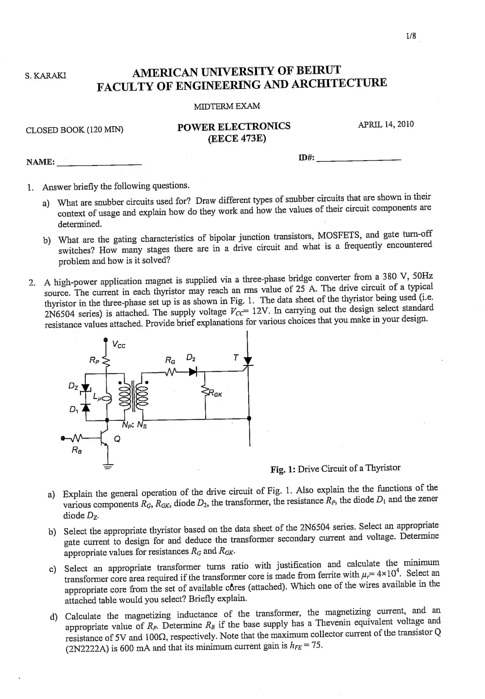
A high-power application magnet is supplied via a three-phase bridge converter from a 380 V, 50Hz
source. The current in each thyristor may reach an rms value of 25 A. The drive circuit of a typical
thyristor in the three-phase set up is as shown in Fig. 1. The data sheet of the thyristor being used (i.e.
2N6504 series) is attached. The supply voltage Vec= 12V. In carrying out the design select standard
resistance values attached. Provide brief explanations for various choices that you make in your design.
C
ReS Ty
Dy Lyle Ws >
of =e t a
Np: Ng
. Q
Voc
Fig. 1: Drive Circuit of a Thyristor
a) Explain the general operation of the drive circuit of Fig. 1. Also explain the the functions of the
various components Rg, Rex, diode D2, the transformer, the resistance Rp, the diode D; and the zener
diode Dz.
b) Select the appropriate thyristor based on the data sheet of the 2N6504 series. Select an appropriate
gate current to design for and deduce the transformer secondary current and voltage. Determine
appropriate values for resistances Rg and Rex.
c) Select an appropriate transformer tums ratio with justification and calculate the minimum
transformer core area required if the transformer core is made from ferrite with = 4x10*. Select an
appropriate core from the set of available cfres (attached). Which one of the wires available in the
attached table would you select? Briefly explain.
d) Calculate the magnetizing inductance of the transformer, the magnetizing current, and an
appropriate value of Rp. Determine R, if the base supply has a Thevenin equivalent voltage and
resistance of 5V and 1002, respectively. Note that the maximum collector current of the transistor Q
(2N2222A) is 600 mA and that its minimum current gain is Arg = 75.
3.
2/8
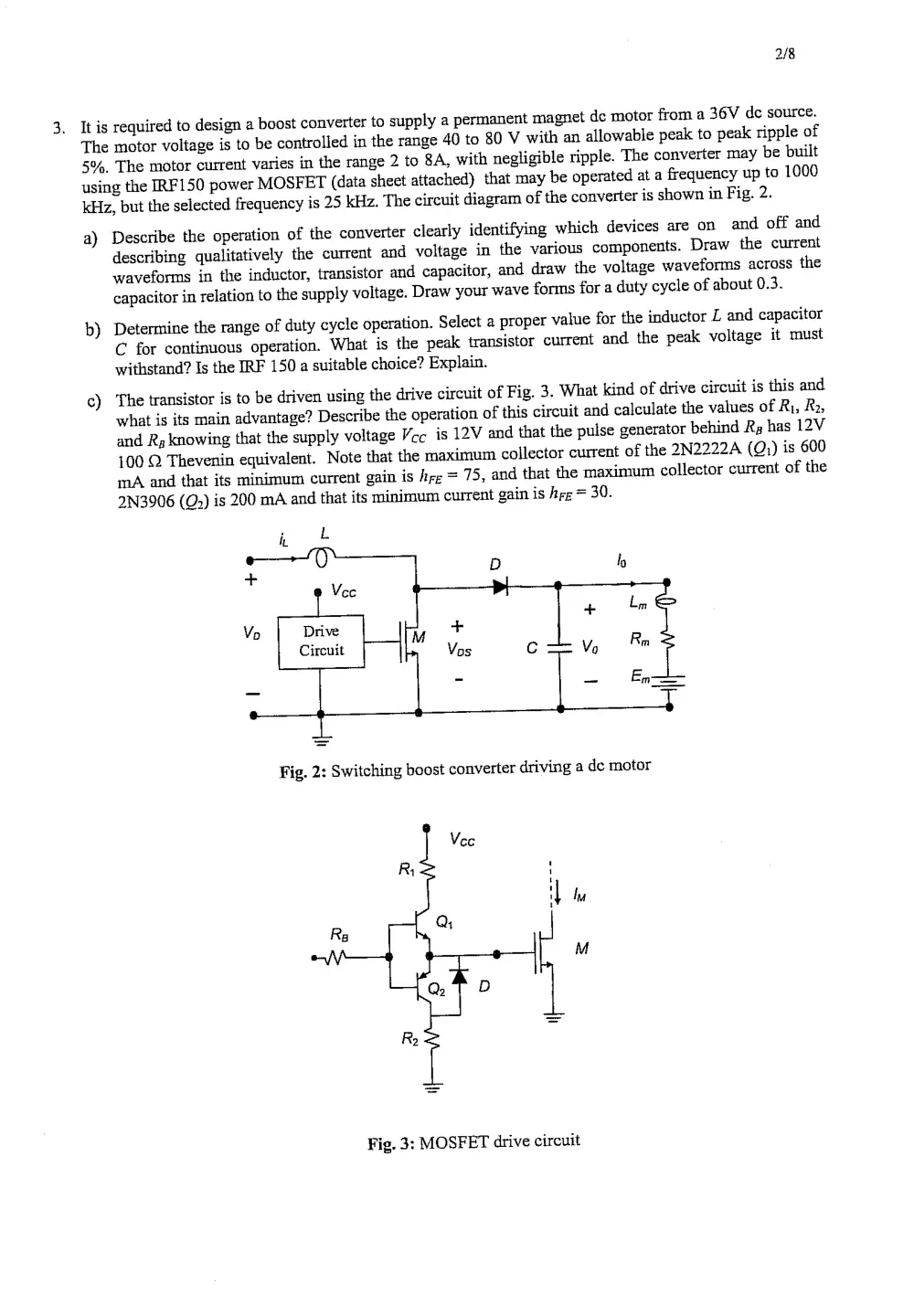
It is required to design a boost converter to supply a permanent magnet de motor from a 36V de source.
The motor voltage is to be controlled in the range 40 to 80 V with an allowable peak to peak ripple of
5%, The motor current varies in the range 2 to 8A, with negligible ripple. The converter may be built
using the IRF150 power MOSFET (data sheet attached) that may be operated at a frequency up to 1000
kHz, but the selected frequency is 25 kHz. The circuit diagram of the converter is shown in Fig. 2.
a) Describe the operation of the converter clearly identifying which devices are on and off and
describing qualitatively the current and voltage in the various components. Draw the current
waveforms in the inductor, transistor and capacitor, and draw the voltage waveforms across the
capacitor in relation to the supply voltage. Draw your wave forms for a duty cycle of about 0.3.
b) Determine the range of duty cycle operation. Select a proper value for the inductor Z and capacitor
C for continuous operation. What is the peak transistor current and the peak voltage it must
withstand? Is the IRF 150 a suitable choice? Explain.
¢) The transistor is to be driven using the drive circuit of Fig. 3. What kind of drive circuit is this and
what is its main advantage? Describe the operation of this circuit and calculate the values of Rj, Ro,
and Ry knowing that the supply voltage Vcc is 12V and that the pulse generator behind R, has 12V
100 Q Thevenin equivalent. Note that the maximum collector current of the 2N2222A (Q)) is 600
mA and that its minimum current gain is hig = 75, and that the maximum collector current of the
2N3906 (Q) is 200 mA and that its minimum current gain is hrg = 30.
lo
D
>| _.
+ bm
+
Vos Cc Vo Rm
- _ En
Drive
Circuit
Fig. 3: MOSFET drive circuit