
EECE 310 Homework 10, Fall 2007
American University of Beirut · Electronics · 2 pages
More EECE 310 files
- Homework Spice2 Solution · Summer 2012Homework · with solutionView
- Homework Spice3 Solution · Summer 2012Homework · with solutionView
- Homework Spice1 Solution · Summer 2012Homework · with solutionView
- Homework 1 Solution · Fall 2011Homework · with solutionView
- Homework 1 · Fall 2011HomeworkView
- Homework 1 · Fall 2011HomeworkView
- Homework 1 Solution · Fall 2011Homework · with solutionView
- Homework 10 · Fall 2011HomeworkView
Show the text of this homework
Page 1 of 2
American University of Beirut
Department of Electrical and Computer Engineering
EECE 310 – Electronics
Fall 2007 – 2008
Homework 10
In the following problems, assume that in the active region, |VBE| = 0.7 V.
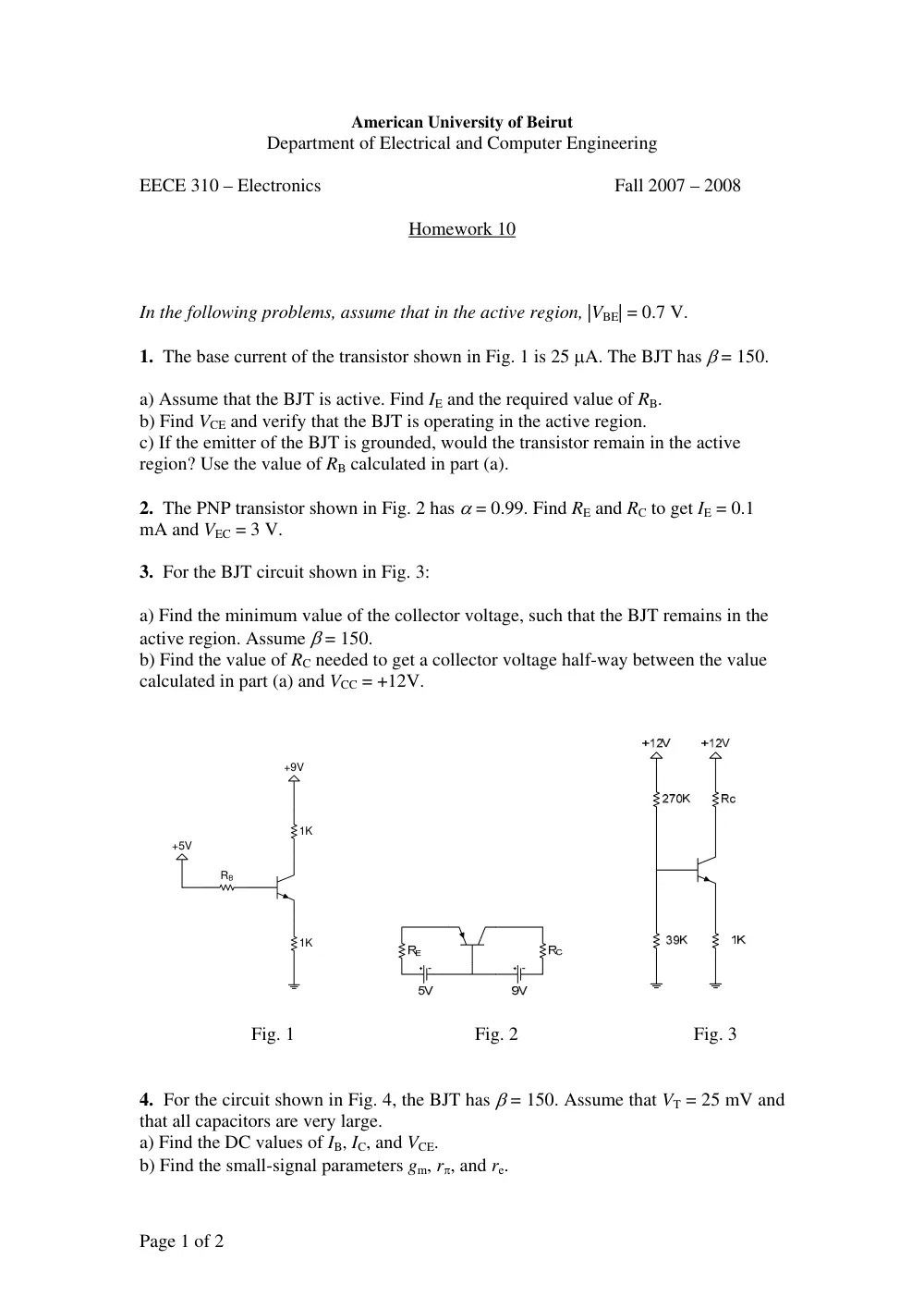
1. The base current of the transistor shown in Fig. 1 is 25 μA. The BJT has β = 150.
a) Assume that the BJT is active. Find IE and the required value of RB.
b) Find VCE and verify that the BJT is operating in the active region.
c) If the emitter of the BJT is grounded, would the transistor remain in the active
region? Use the value of RB calculated in part (a).
2. The PNP transistor shown in Fig. 2 has α = 0.99. Find RE and RC to get IE = 0.1
mA and VEC = 3 V.
3. For the BJT circuit shown in Fig. 3:
a) Find the minimum value of the collector voltage, such that the BJT remains in the
active region. Assume β = 150.
b) Find the value of RC needed to get a collector voltage half-way between the value
calculated in part (a) and VCC = +12V.
+9V
1K
1K
RB
+5V
Fig. 1
Fig. 2
Fig. 3
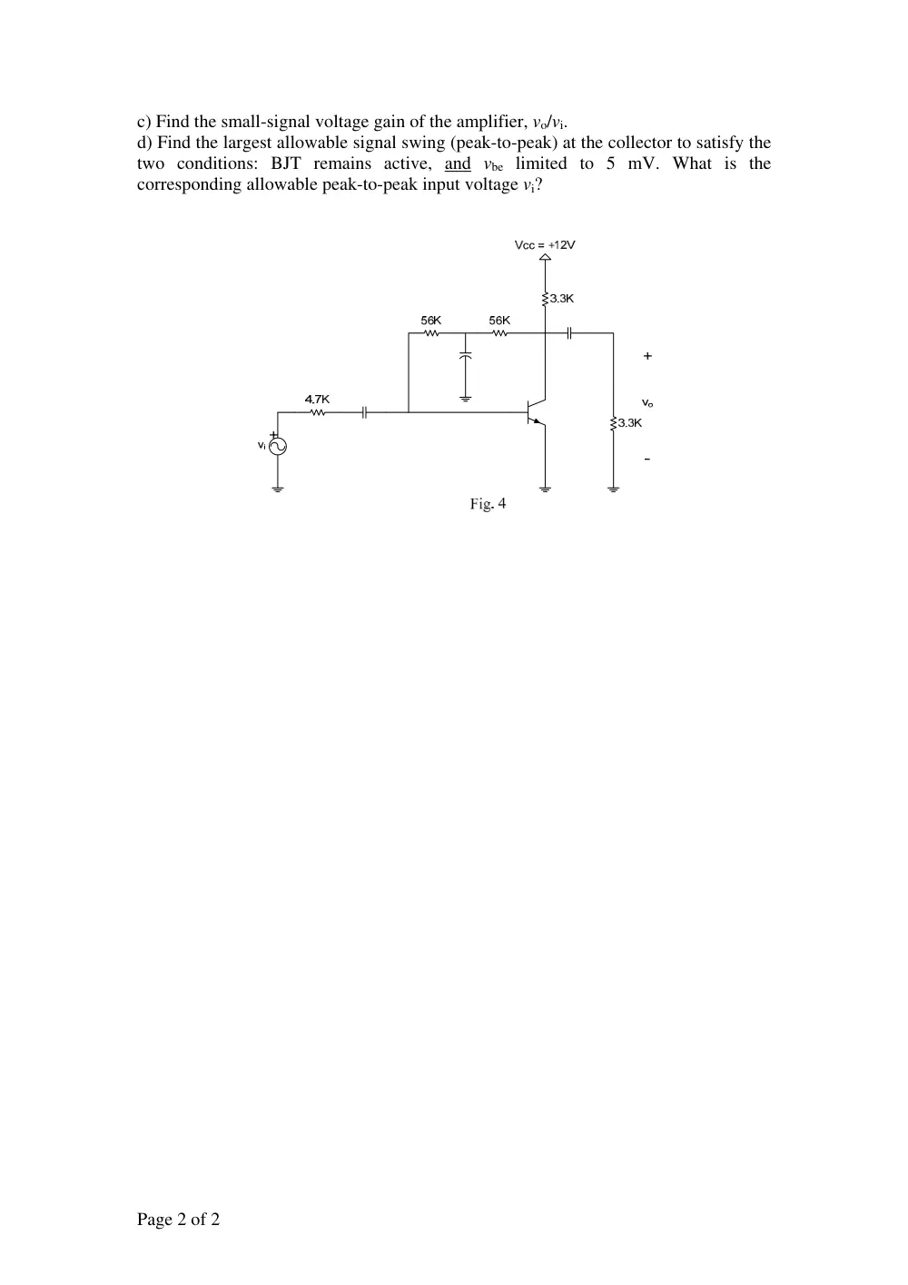
4. For the circuit shown in Fig. 4, the BJT has β = 150. Assume that VT = 25 mV and
that all capacitors are very large.
a) Find the DC values of IB, IC, and VCE.
b) Find the small-signal parameters gm, rπ, and re.
Page 2 of 2
c) Find the small-signal voltage gain of the amplifier, vo/vi.
d) Find the largest allowable signal swing (peak-to-peak) at the collector to satisfy the
two conditions: BJT remains active, and vbe limited to 5 mV. What is the
corresponding allowable peak-to-peak input voltage vi?