
EECE 320 Midterm, Fall 2005
American University of Beirut · Digital Systems Design · 11 pages


Showing the first 10 of 11 pages. Download the PDF to see all of it.
More EECE 320 files
Show the text of this exam
M. MANSOUR
DEPARTMENT OF ELECTRICAL AND COMPUTER EGINEERING
AMERICAN UNIVERSITY OF BEIRUT
FALL TERM 2005-2006
MIDTERM II
EECE320 - DIGITAL SYTEMS DESIGN
December 19, 2005
UNAMEU: _____________________
ID: _____________________
UCOURSE SECTIONU: SECTIONS 2 & 3 (PROF. MANSOUR)
INSTRUCTIONS:
o BE AS NEAT AND CLEAR AS POSSIBLE.
o INDICATE THE SECTION YOU ARE REGISTERED IN.
o PROVIDE YOUR ANSWERS IN THE SPACE PROVIDED ON THE QUESTION SHEET.
o THE SCRATCH BOOKLET UWILL NOTU BE CONSIDERED IN GRADING.
o WRITE YOUR NAME AND ID NUMBER IN THE SPACE PROVIDED ABOVE.
o CALCULATORS ARE NOT ALLOWED.
o THE EXAM IS CLOSED BOOK/CLOSED NOTES. THE DURATION IS U1.5 HOURSU.
Problem
Total Points
Earned Points
1
12
2
12
3
12
4
10
5
12
6
20
7
10
8
12
Total
100
Page 1 of 11
UProblem 1U: AND-XOR Canonical Form [12 points]
Let F(a, b) be a Boolean function of two variables. We know that F can be written as a canonical sum-of-
product as follows:
)1,1(
)
0,1(
)1,0
(
( 0,0 )
( , )
a b F
a b F
a b F
a b F
F a b
⋅ ⋅
+
⋅ ⋅
+
⋅ ⋅
+
⋅ ⋅
=
An alternative canonical form of writing F is using only AND and XOR functions. Show how to express
F using only AND and XOR functions. HINT: each of the above product terms is a min-term, what
property do the min-terms have in common and how is that useful for XOR functions?
USolutionU:
Since the above expression has terms which are mutually exclusive (minterms, ‘+’ can be
replaced by
⊕
)1,1(
)1,0
(
. . ( 0,0 )
( , )
ab F
ab F
a b F
F a b
⊕
⊕
=
⇒
the inverted variables
( . . )
e g a
can be replaced with
⊕1
a
Page 2 of 11
UProblem 2U: Combinational Shifter [12 points]
Design a combinational logic circuit with 8 data inputs AB1
B, AB2
B, …, AB8
B, three control inputs SB2
B, SB1
B, SB0
B,
and 8 outputs OB1
B, OB2
B, …, OB8
B.The output word is equal to the input word, rotated to the right circularly
by a number of bit positions specified by the control inputs. For example, if the input word is 10111010
and the control inputs are 011, then the output word is 01010111. Label your inputs and outputs clearly.
USolutionU:
S2
S1
S0
0
0
0
no rotation
0
0
1
1
0
1
0
2
0
1
1
3
1
0
0
4
1
0
1
5
1
1
0
6
1
1
1
7
OB8
B
O
7 6 5 4 3 2 1 0
AB2
B AB1
B AB8
B AB3
B
SB1
B
SB2
B
SB0
B
OB3
B
. . .
7 6 5 4 3 2 1 0
AB7
B AB6
B AB1
B AB8
B
SB1
B
SB2
B
SB0
B
OB4
B
. . .
7 6 5 4 3 2 1 0
AB8
B AB7
B AB2
B AB1
B
SB1
B
SB2
B
SB0
B
OB1
B
. . .
7 6 5 4 3 2 1 0
AB1
B AB8
B AB3
B AB2
B
SB1
B
SB2
B
SB0
B
OB2
B
. . .
Page 3 of 11
UProblem 3U: MN Flip Flop [12 points]
A MN flip-flop has two inputs M and N, and outputs Q and Q’. Input M behaves like the complement of
the J input of a JK flip-flop, and input N behaves like the K input of a JK flip-flop.
(a)
Obtain the characteristic equation of the MN flip-flop. [2 points]
M=J’
N=K
Q*=Q'M' + QN'
M
N
Q Q*
0
0
1
0
1
last Q'
1
0
last Q
1
1
0
Q MN
00
00
00
00
0
1
1
1
1
1
1
1
1
1
(b)
Complete the following table for the MN flip-flop. You must specify the appropriate values
to be applied on M and N to obtain the corresponding transition from Q to Q*. [4 points]
M
N
Q
Q*
0
0
0
1
0
0
1
1
0
1
0
1
0
1
1
0
1
0
0
0
1
0
1
1
1
1
0
0
1
1
1
0
Current State
Next State
Inputs to be applied
Q
Q*
M
N
0
0
1
d
0
1
0
d
1
0
d
1
1
1
d
0
(c)
Design a D flip-flop using an MN flip-flop. [3 points]
(d)
Design an MN flip-flop using a D flip-flop. [3 points]
Q
N
M
Q’
D
CLK
CLK
D
Q
M
N
Page 4 of 11
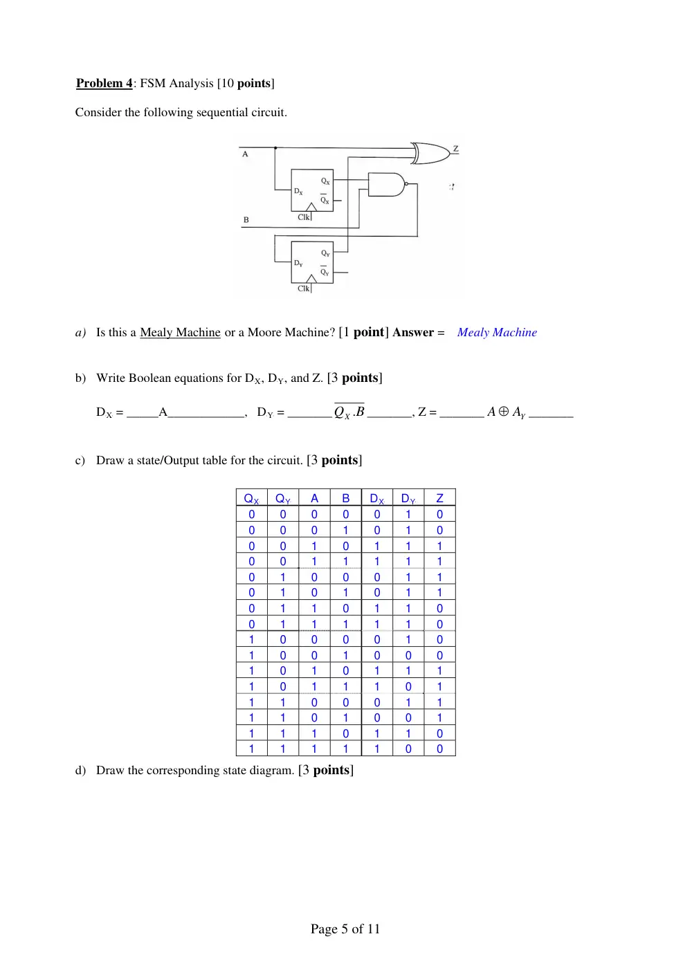
UProblem 4U: FSM Analysis [10 points]
Consider the following sequential circuit.
a) Is this a UMealy MachineU or a Moore Machine? [1 point] Answer = Mealy Machine
b) Write Boolean equations for DBX
B, DBY
B, and Z. [3 points]
DBX
B = _____A____________, DBY
B = _______
QX .B
_______, Z = _______
AY _______
A ⊕
c) Draw a state/Output table for the circuit. [3 points]
QBX
B
QBY
B
A
B
DBX
B
DBY
B
Z
0
0
0
0
0
1
0
0
0
0
1
0
1
0
0
0
1
0
1
1
1
0
0
1
1
1
1
1
0
1
0
0
0
1
1
0
1
0
1
0
1
1
0
1
1
0
1
1
0
0
1
1
1
1
1
0
1
0
0
0
0
1
0
1
0
0
1
0
0
0
1
0
1
0
1
1
1
1
0
1
1
1
0
1
1
1
0
0
0
1
1
1
1
0
1
0
0
1
1
1
1
0
1
1
0
1
1
1
1
1
0
0
d) Draw the corresponding state diagram. [3 points]
Page 5 of 11
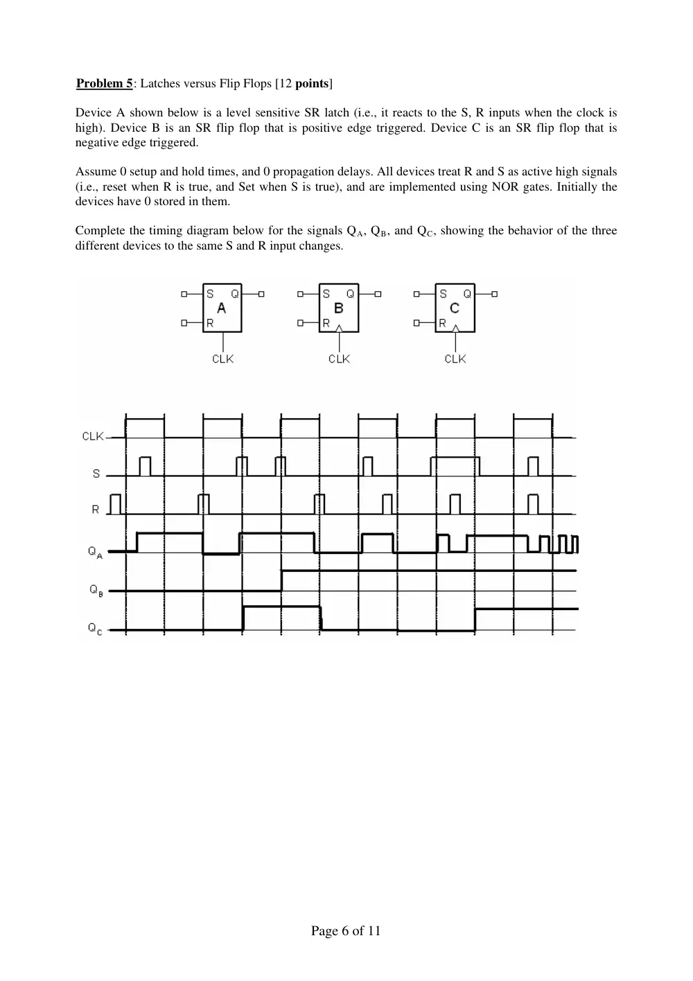
UProblem 5U: Latches versus Flip Flops [12 points]
Device A shown below is a level sensitive SR latch (i.e., it reacts to the S, R inputs when the clock is
high). Device B is an SR flip flop that is positive edge triggered. Device C is an SR flip flop that is
negative edge triggered.
Assume 0 setup and hold times, and 0 propagation delays. All devices treat R and S as active high signals
(i.e., reset when R is true, and Set when S is true), and are implemented using NOR gates. Initially the
devices have 0 stored in them.
Complete the timing diagram below for the signals QBA
B, QBB
B, and QBC
B, showing the behavior of the three
different devices to the same S and R input changes.
Page 6 of 11
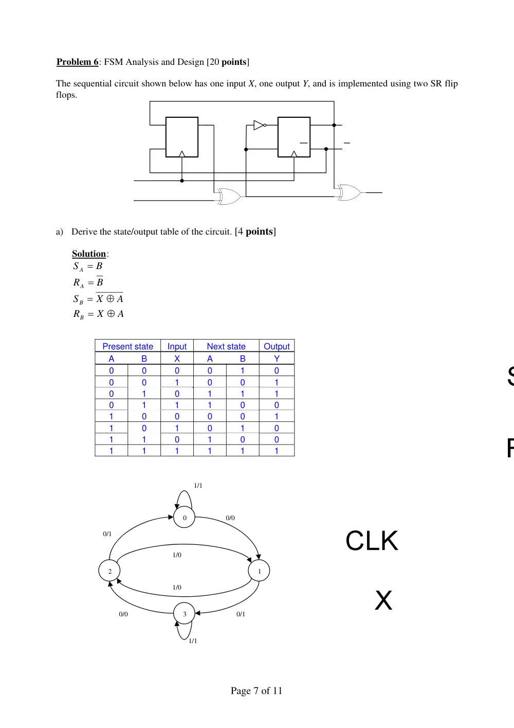
UProblem 6U: FSM Analysis and Design [20 points]
The sequential circuit shown below has one input X, one output Y, and is implemented using two SR flip
flops.
a) Derive the state/output table of the circuit. [4 points]
USolutionU:
S A = B
RA = B
A
X
S B
⊕
=
A
X
RB
⊕
=
Present state
Input
Next state
Output
A
B
X
A
B
Y
0
0
0
0
1
0
0
0
1
0
0
1
0
1
0
1
1
1
0
1
1
1
0
0
1
0
0
0
0
1
1
0
1
0
1
0
1
1
0
1
0
0
1
1
1
1
1
1
0
1/1
1
3
2
0/0
0/1
0/0
1/1
1/0
1/0
0/1
Page 7 of 11
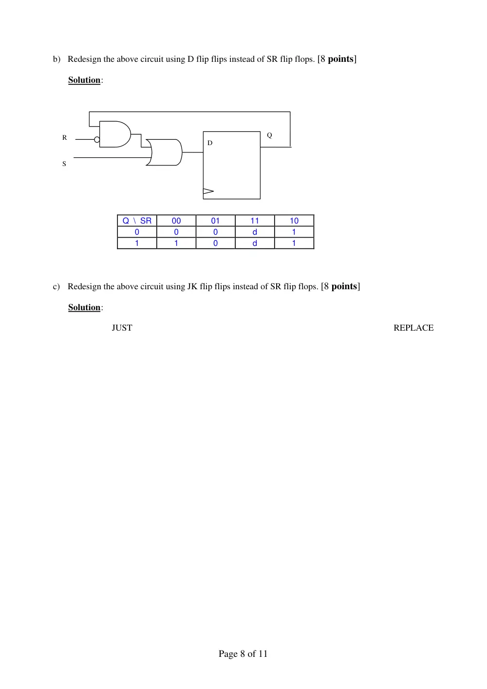
b) Redesign the above circuit using D flip flips instead of SR flip flops. [8 points]
USolutionU:
Q
Q \ SR
00
01
11
10
0
0
0
d
1
1
1
0
d
1
c) Redesign the above circuit using JK flip flips instead of SR flip flops. [8 points]
USolutionU:
JUST
REPLACE
R
D
S
Page 8 of 11
UProblem 7U: Serial 2’s Complementer [10 points]
A serial two’s complementer is to be designed. A binary integer of arbitrary length is presented to the
serial two’s complementer, least significant bit first, on input X. When a given bit is presented on input
X, the corresponding output bit is to appear during the same clock cycle on output Z. To indicate that a
sequence is complete and that the circuit is to be initialized to receive another sequence, input Y becomes
1 for one clock cycle. Otherwise, Y is 0. Draw the state diagram for the two’s complementer circuit.
Identify the meaning of each state in your diagram.
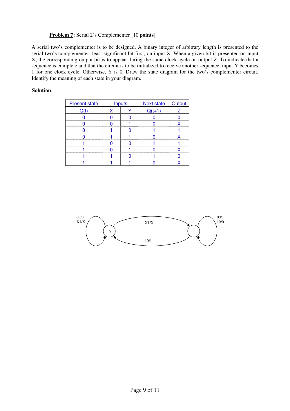
USolutionU:
Present state
Inputs
Next state
Output
Q(t)
X
Y
Q(t+1)
Z
0
0
0
0
0
0
0
1
0
X
0
1
0
1
1
0
1
1
0
X
1
0
0
1
1
1
0
1
0
X
1
1
0
1
0
1
1
1
0
X
1
0
00/1
10/0
10/1
X1/X
00/0
X1/X
Page 9 of 11
UProblem 8U: FSM Design [12 points]
A sequential circuit has three flip flops A, B, C; one input x; one output y. The state diagram is shown
below. The circuit is to be designed by treating the unused states as don’t cares. Design the FSM using D
flip flops.
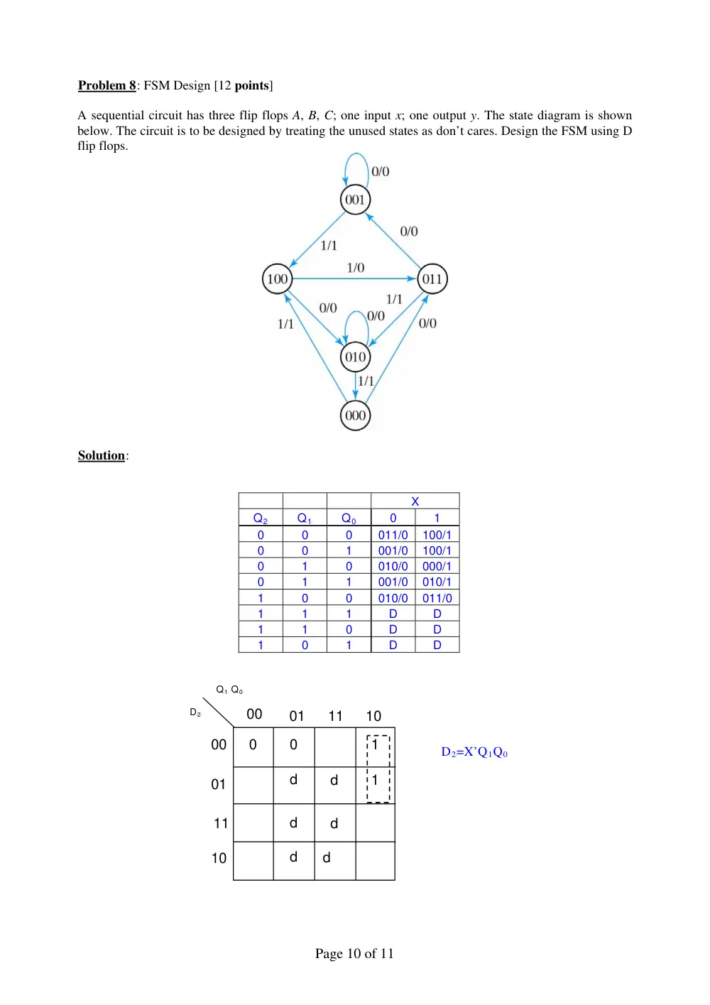
USolutionU:
X
QB2
B
QB1
B
QB0
B
0
1
0
0
0
011/0
100/1
0
0
1
001/0
100/1
0
1
0
010/0
000/1
0
1
1
001/0
010/1
1
0
0
010/0
011/0
1
1
1
D
D
1
1
0
D
D
1
0
1
D
D
DB2
B=X’QB1
BQB0
DB2
B
QB1
B QB0
B
00
01
11
10
00
0
1
0
01
11
10
d
d
d
d
d
d
1
Page 10 of 11
D1=QB0
B+QB2
B’QB1
B’+XQB2
BQB1
B
XQB2
B
QB1
B QB0
B
00
01
11
10
00
1
1
1
01
11
10
d
d
d
d
d
1
d
1
DB0
B=QB2
BQB1
B’+X’QB1
B’QB0
B’+QB1
BQB0
B
XQB2
B
QB1
B QB0
B
00
01
11
10
00
01
11
10
d
d
1
d
d
1
d
d
1
1
1
Page 11 of 11