
EECE 320 Midterm Solution, Fall 2004
American University of Beirut · Digital Systems Design · 11 pages · with solution




Showing the first 10 of 11 pages. Download the PDF to see all of it.
More EECE 320 files
Show the text of this exam
EECE 320 – Digital Systems Design
Fall 2004
Midterm Solution
Problem 1: [20 points]
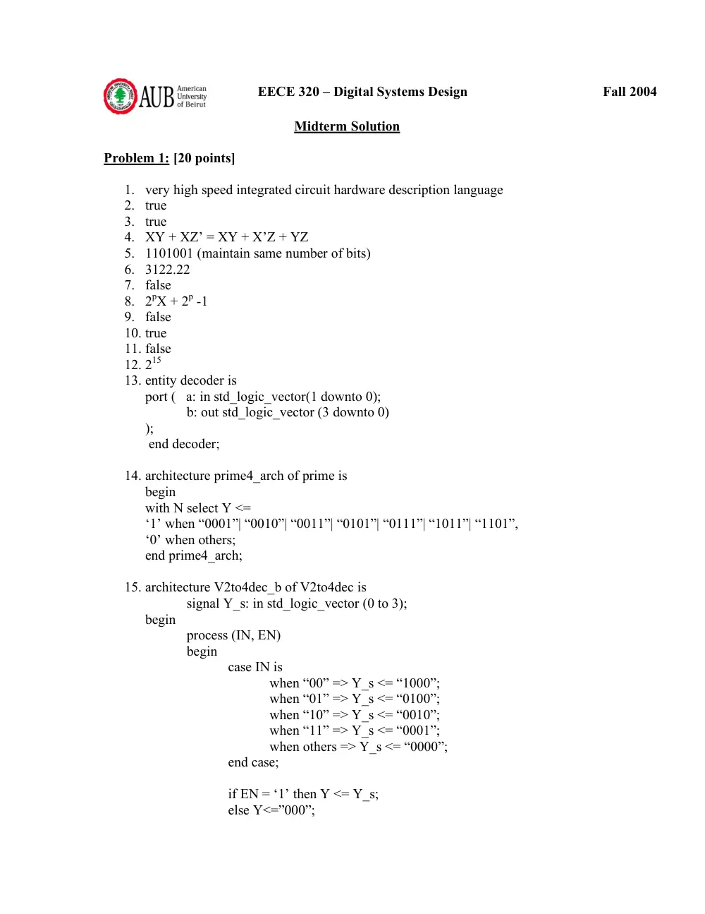
1. very high speed integrated circuit hardware description language
2. true
3. true
4. XY + XZ’ = XY + X’Z + YZ
5. 1101001 (maintain same number of bits)
6. 3122.22
7. false
8. 2pX + 2p -1
9. false
10. true
11. false
12. 215
13. entity decoder is
port ( a: in std_logic_vector(1 downto 0);
b: out std_logic_vector (3 downto 0)
);
end decoder;
14. architecture prime4_arch of prime is
begin
with N select Y <=
‘1’ when “0001”| “0010”| “0011”| “0101”| “0111”| “1011”| “1101”,
‘0’ when others;
end prime4_arch;
15. architecture V2to4dec_b of V2to4dec is
signal Y_s: in std_logic_vector (0 to 3);
begin
process (IN, EN)
begin
case IN is
when “00” => Y_s <= “1000”;
when “01” => Y_s <= “0100”;
when “10” => Y_s <= “0010”;
when “11” => Y_s <= “0001”;
when others => Y_s <= “0000”;
end case;
if EN = ‘1’ then Y <= Y_s;
else Y<=”000”;
end if;
end process;
end V2to4dec_b;
16. FD = (X’ + Y’ + Z)(X’ + Y + Z)(X + Y’ + Z)(X + Y + Z)
= ∏(0,2,4,6) = F
(it turns out that F is self dual)
17. possibility of a circuit producing a 0 glitch when the output is expected to remain
at 1
18. 1
19. minimal sum is a sum of prime implicants
20. adjacent number differ by exactly one bit
Problem 2: [8 points]
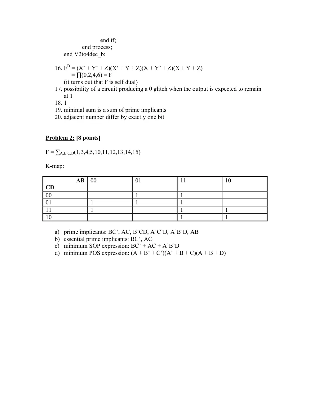
F = ∑A,B,C,D(1,3,4,5,10,11,12,13,14,15)
K-map:
AB
CD
00
01
11
10
00
1
1
01
1
1
1
11
1
1
1
10
1
1
a) prime implicants: BC’, AC, B’CD, A’C’D, A’B’D, AB
b) essential prime implicants: BC’, AC
c) minimum SOP expression: BC’ + AC + A’B’D
d) minimum POS expression: (A + B’ + C’)(A’ + B + C)(A + B + D)
Problem 3: [6 points]
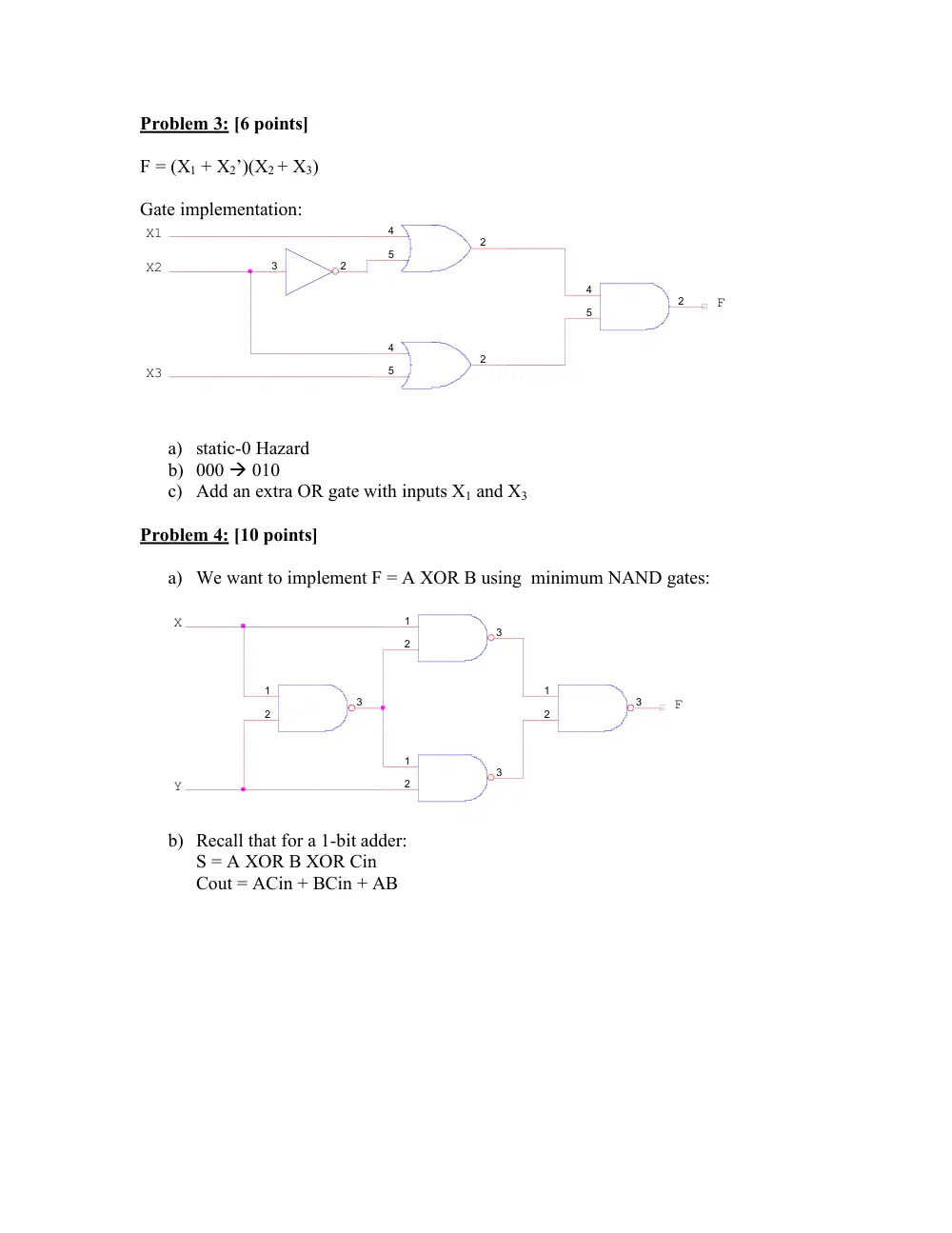
F = (X1 + X2’)(X2 + X3)
Gate implementation:
X1
4
5
2
X2
3
2
4
5
2
X3
F
4
5
2
a) static-0 Hazard
b) 000 010
c) Add an extra OR gate with inputs X1 and X3
Problem 4: [10 points]
a) We want to implement F = A XOR B using minimum NAND gates:
1
2
3
Y
1
2
3
X
F
1
2
3
1
2
3
b) Recall that for a 1-bit adder:
S = A XOR B XOR Cin
Cout = ACin + BCin + AB
F1 = XY
F2 = X + Y
F3 = X XOR Y
F4 = X XNOR Y
F5 = X’
F6 = X XNOR Y XNOR Z
Problem 5: [10 points]
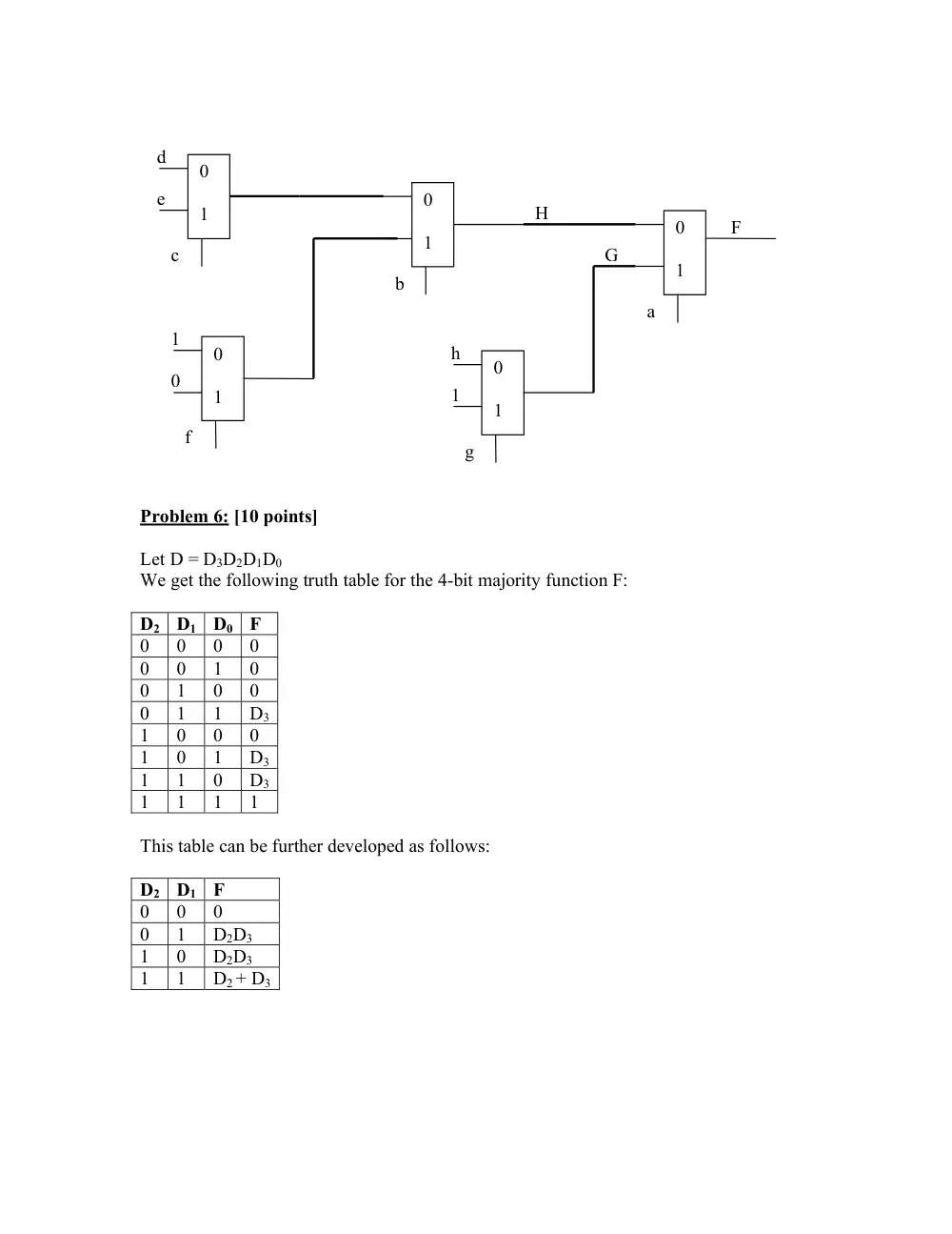
F(a,b,c,d,e,f,g,h) = a’b’c’d + ag’h + ag + a’b’ce + a’bf ’
So F = aF(a = 1) + a’F(a = 0) by Shannon’s theorem
F (a = 1) = g’h + g = G
F (a = 0) = b’c’d + b’ce + bf’ = H
G = g(1) + g’h: implemented using a mux having inputs 1 and h and select signal g
H(b,c,d,e,f) = bH(b = 1) + b’H(b = 0): mux with inputs H(b = 1) and H(b = 0) and select
signal b
H(b = 1) = f’ = f(0) + f’(1): mux with inputs 0 and 1 and select signal f
H(b = 0) = c’d + ce: mux with inputs d and e and select signal c
FA
FA
FA
1
F4
Y
X
1
F5
Y
Z
F6
X
0
X
FA
FA
FA
0
F1
Y
X
1
F2
Y
0
F3
X
Y
X
Problem 6: [10 points]
Let D = D3D2D1D0
We get the following truth table for the 4-bit majority function F:
D2 D1 D0 F
0
0
0
0
0
0
1
0
0
1
0
0
0
1
1
D3
1
0
0
0
1
0
1
D3
1
1
0
D3
1
1
1
1
This table can be further developed as follows:
D2 D1 F
0
0
0
0
1
D2D3
1
0
D2D3
1
1
D2 + D3
0
1
d
e
c
0
1
b
c
0
1
1
0
f
0
1
h
1
g
0
1
a
H
G
F
We obtain the following logic circuit:
Problem 7: [8 points]
a)
b)
Problem 8: [10 points]
LUT
d = 0
e = 0
a
b
LUT
d = 0
e = 1
a
b
LUT
d = 1
e = 0
a
b
LUT
d = 1
e = 1
a
b
c
c
c
c
00
01
MUX
10
11
d e
G
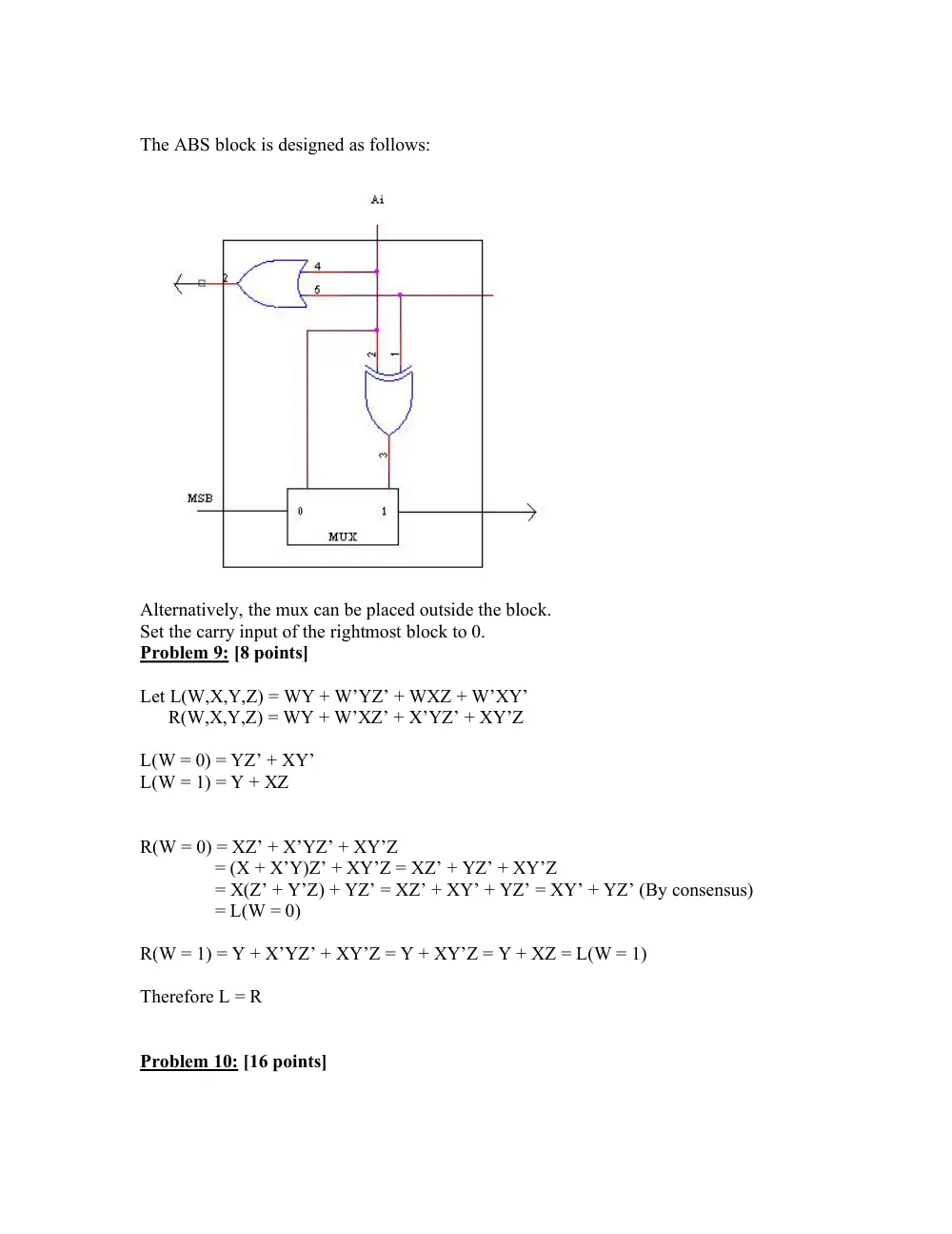
The ABS block is designed as follows:
Alternatively, the mux can be placed outside the block.
Set the carry input of the rightmost block to 0.
Problem 9: [8 points]
Let L(W,X,Y,Z) = WY + W’YZ’ + WXZ + W’XY’
R(W,X,Y,Z) = WY + W’XZ’ + X’YZ’ + XY’Z
L(W = 0) = YZ’ + XY’
L(W = 1) = Y + XZ
R(W = 0) = XZ’ + X’YZ’ + XY’Z
= (X + X’Y)Z’ + XY’Z = XZ’ + YZ’ + XY’Z
= X(Z’ + Y’Z) + YZ’ = XZ’ + XY’ + YZ’ = XY’ + YZ’ (By consensus)
= L(W = 0)
R(W = 1) = Y + X’YZ’ + XY’Z = Y + XY’Z = Y + XZ = L(W = 1)
Therefore L = R
Problem 10: [16 points]
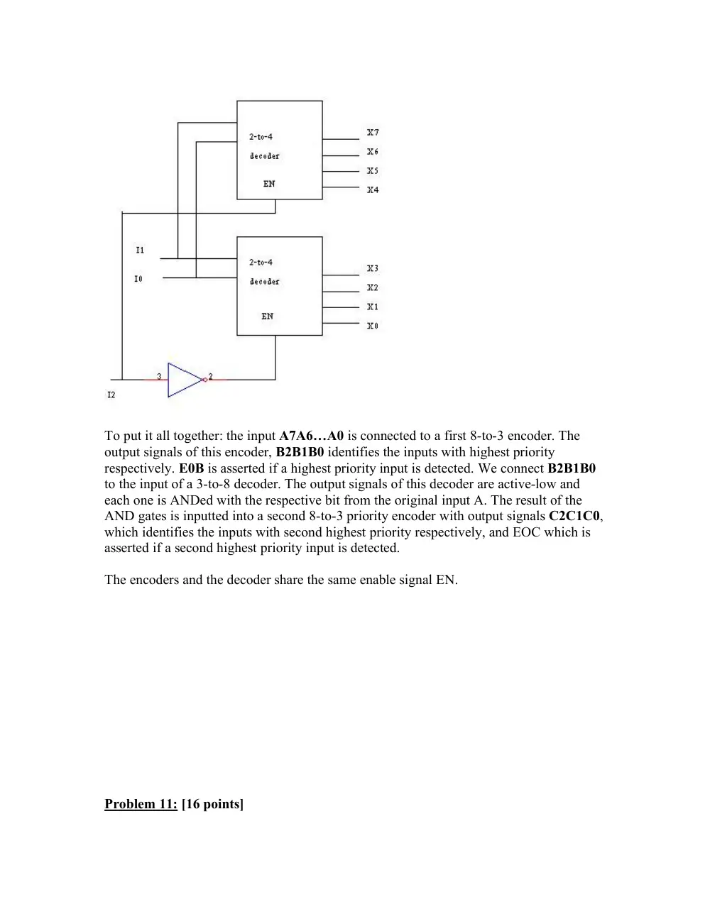
We first build the 8-to-3 encoder from 4-to-2 encoders, and 3-to-8 decoders from 2-to-4
decoders.
8-3 encoder:
3-8 decoder:
To put it all together: the input A7A6…A0 is connected to a first 8-to-3 encoder. The
output signals of this encoder, B2B1B0 identifies the inputs with highest priority
respectively. E0B is asserted if a highest priority input is detected. We connect B2B1B0
to the input of a 3-to-8 decoder. The output signals of this decoder are active-low and
each one is ANDed with the respective bit from the original input A. The result of the
AND gates is inputted into a second 8-to-3 priority encoder with output signals C2C1C0,
which identifies the inputs with second highest priority respectively, and EOC which is
asserted if a second highest priority input is detected.
The encoders and the decoder share the same enable signal EN.
Problem 11: [16 points]
Entity comp1 is
port (
A, B: in std_logic;
EQi: in std_logic;
EQo : out std_logic);
End comp1;
Architecture comp1 of comp1 is
Signal X, XN: std_logic;
Begin
X<= A XOR B;
XN <= NOT X;
EQo <= EQi AND XN;
End comp1;
Entity comp8 is
Port (
A,B: in std_logic_vector(7 downto 0);
EQi: in std_logic;
EQo: out std_logic);
End comp8;
Architecture comp8 of comp8 is
Signal EQ: std_logic_vector(8 downto 0);
Component comp1
port (
A, B: in std_logic;
EQi: in std_logic;
EQo : out std_logic);
End component;
Begin
For i in 0 to 7 generate
U1: comp port map (A(i), B(i), EQ(i), EQ(i + 1));
End generate;
EQ(0) <= EQi;
EQo <= EQ(8);
End comp8;
Testbench:
Plug in the following values:
A<=0x”23”; B<=0x”32”; wait for 10 ns;
A<=0x”34”; B<=0x”34”; wait for 10 ns;
A<=0x”FF”; B<=0x”00”; wait for 10 ns;