
EECE 310 Exam 1, Fall 2004
American University of Beirut · Electronics · 10 pages

More EECE 310 files
- Midterm · Fall 2014ExamView
- Midterm with Solutions · Fall 2014Exam · with solutionView
- Midterm · Fall 2013ExamView
- Midterm · Fall 2012ExamView
- Exam 2 with Answers · Fall 2011Exam · with solutionView
- Exam 1 with Answers · Fall 2011Exam · with solutionView
- Midterm with Solution · Summer 2011Exam · with solutionView
- Exam 1 · Fall 2010ExamView
Show the text of this exam
EECE 310 – Quiz 1 – Fall 2004/2005 – Page 1 of 10
American University of Beirut
P1 /16
Department of Electrical and Computer Engineering
P2 /12
EECE 310 – Electronics I
P3 /12
Fall 2004 – 2005
P4 /12
Quiz 1 – November 5, 2004
P5 /6
Closed Book – 90 minutes
P6 /12
P7 /10
P8 /10
P9 /10
Grade /100
NAME:___________________________ ID Number: ______________________
I have neither given nor received aid on this exam
SIGNATURE
ASSUME VT = 25 mV, UNLESS OTHERWISE SPECIFIED
Problem 1 [16 points]
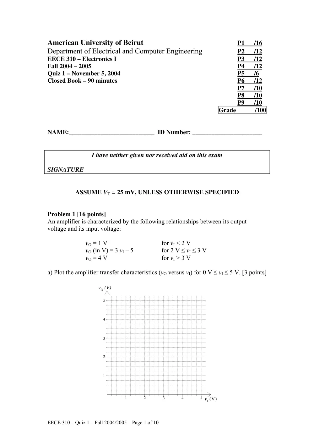
An amplifier is characterized by the following relationships between its output
voltage and its input voltage:
vO = 1 V
for vI < 2 V
vO (in V) = 3 vI – 5
for 2 V ≤ vI ≤ 3 V
vO = 4 V
for vI > 3 V
a) Plot the amplifier transfer characteristics (vO versus vI) for 0 V ≤ vI ≤ 5 V. [3 points]
vI (V)
vO (V)
5
1
1
2
3
4
2
3
4
5
EECE 310 – Quiz 1 – Fall 2004/2005 – Page 2 of 10
b) In the amplification region, what is the gain of the amplifier (in V/V)? What is the
gain of the amplifier in dB? [3 points]
c) What is the maximum peak-to-peak undistorted variation in the output voltage?
What is the corresponding peak-to-peak variation in the input voltage? [3 points]
d) Where should the bias point (VI, VO) of this amplifier be in order to get the
maximum undistorted output? [3 points]
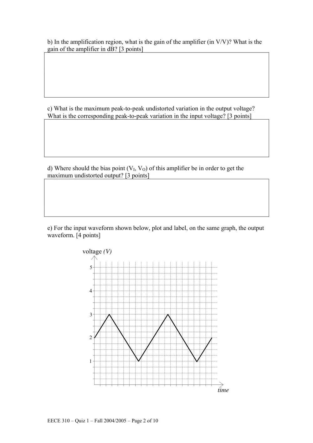
e) For the input waveform shown below, plot and label, on the same graph, the output
waveform. [4 points]
time
voltage (V)
1
2
3
4
5
EECE 310 – Quiz 1 – Fall 2004/2005 – Page 3 of 10
Problem 2 [12 points]
Measurements on a Si diode were taken at vD = 0.35 V, 0.45 V, 0.55 V, and 0.65 V.
The natural logarithm of the diode current in Amps, ln(iD), is plotted on the y-axis
versus vD in Volts, on the x-axis. The resulting straight-line has a slope of 32, and a y-
axis intercept of –30.
a) For this diode, find the values of n and IS. [8 points]
b) What is the diode current when vD = 0.7 V? [4 points]
EECE 310 – Quiz 1 – Fall 2004/2005 – Page 4 of 10
Problem 3 [12 points]
The diodes in the circuit shown drop 0.7 V when conducting.
Calculate the current in D2 and the voltage across R3. Verify all your assumptions.
15 V
15 V
R1 = 5K
R2 = 10K
R3 = 10K
D1
D2
R4 = 5K
EECE 310 – Quiz 1 – Fall 2004/2005 – Page 5 of 10
Problem 4 [12 points]
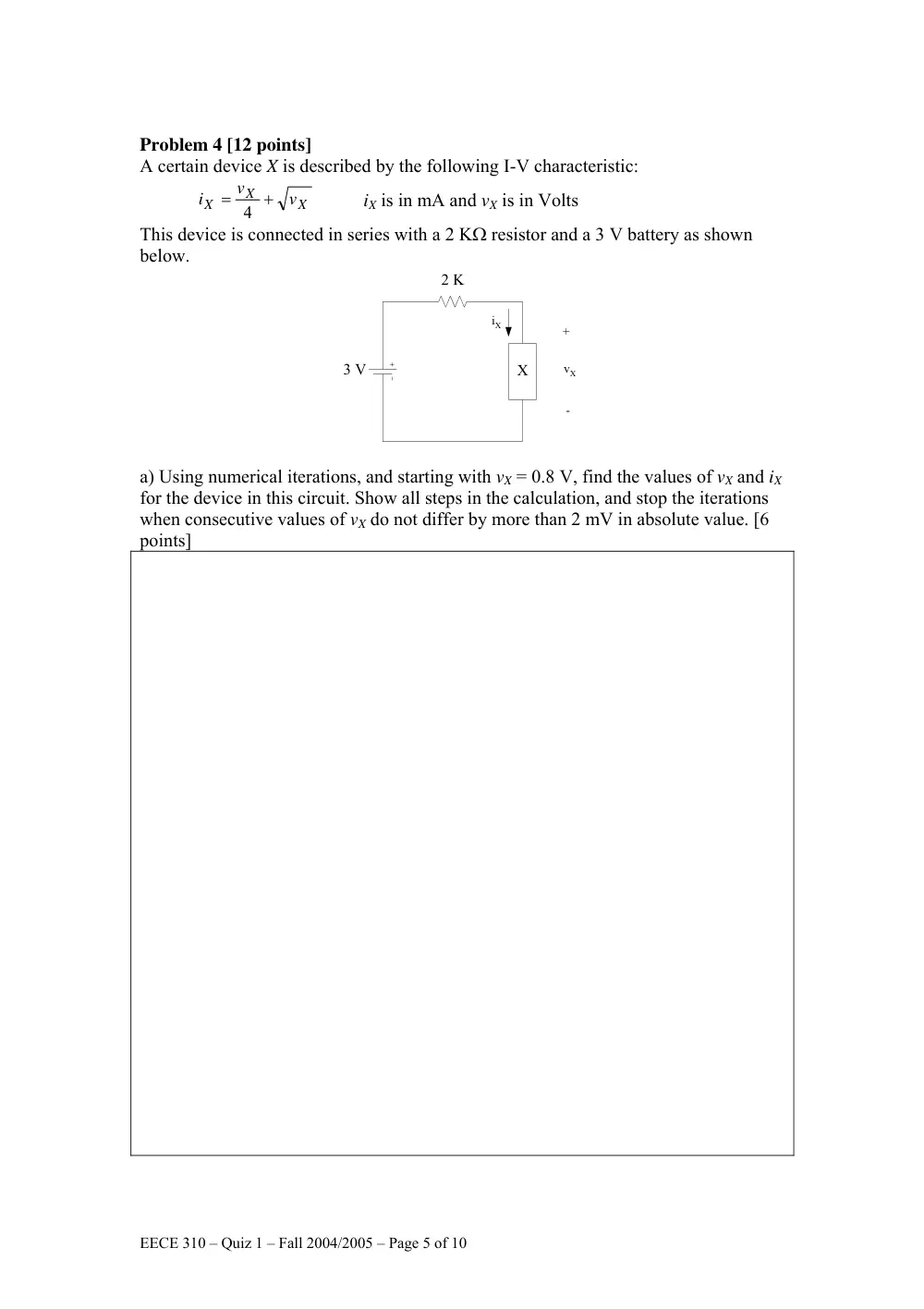
A certain device X is described by the following I-V characteristic:
X
X
X
v
v
i
= 4 +
iX is in mA and vX is in Volts
This device is connected in series with a 2 KΩ resistor and a 3 V battery as shown
below.
3 V
2 K
X
iX
vX
+
-
a) Using numerical iterations, and starting with vX = 0.8 V, find the values of vX and iX
for the device in this circuit. Show all steps in the calculation, and stop the iterations
when consecutive values of vX do not differ by more than 2 mV in absolute value. [6
points]
EECE 310 – Quiz 1 – Fall 2004/2005 – Page 6 of 10
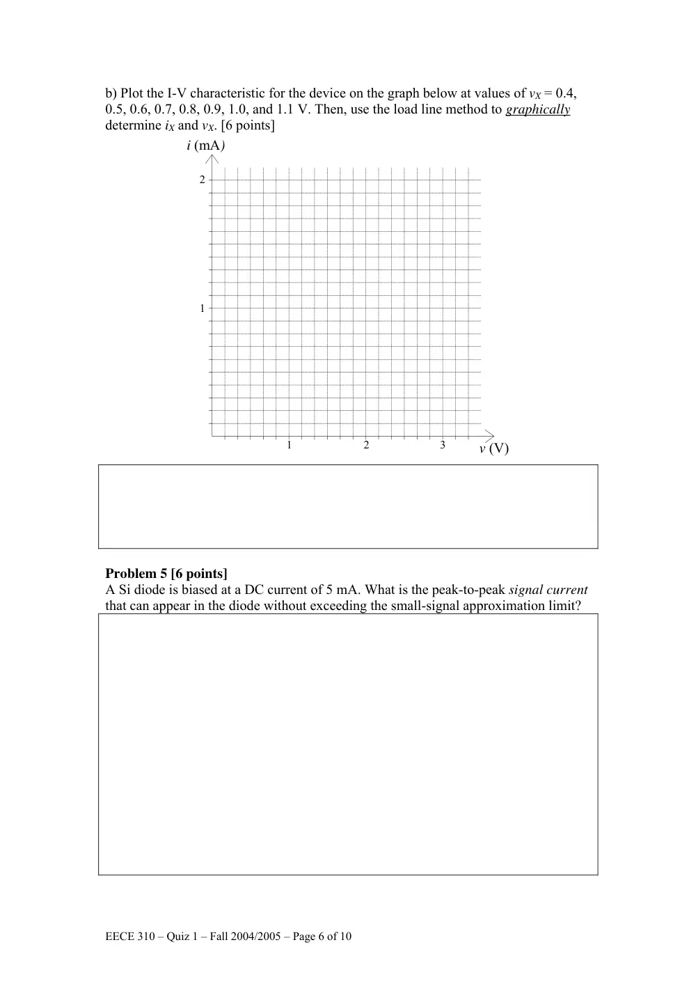
b) Plot the I-V characteristic for the device on the graph below at values of vX = 0.4,
0.5, 0.6, 0.7, 0.8, 0.9, 1.0, and 1.1 V. Then, use the load line method to graphically
determine iX and vX. [6 points]
v (V)
i (mA)
2
1
1
2
3
Problem 5 [6 points]
A Si diode is biased at a DC current of 5 mA. What is the peak-to-peak signal current
that can appear in the diode without exceeding the small-signal approximation limit?
EECE 310 – Quiz 1 – Fall 2004/2005 – Page 7 of 10
Problem 6 [12 points]
A full-wave rectifier with a center-tap transformer uses two diodes that are assumed
ideal. The average value of the output voltage is 10 V, across a 100 Ω load resistor.
a) Find the maximum value of the sinusoidal voltage at the secondary of the
transformer (from the center tap to one of the transformer terminals on the secondary.)
[4 points]
b) Find the average diode current. [4 points]
c) Find the diode PIV. [4 points]
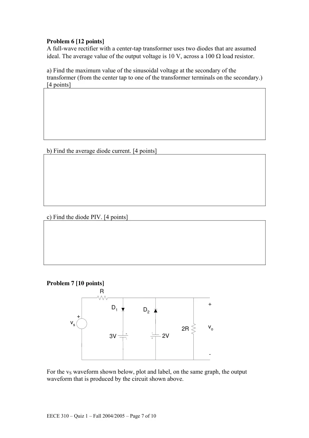
Problem 7 [10 points]
R
+
2V
vo
+
-
vs
3V
2R
D1
D2
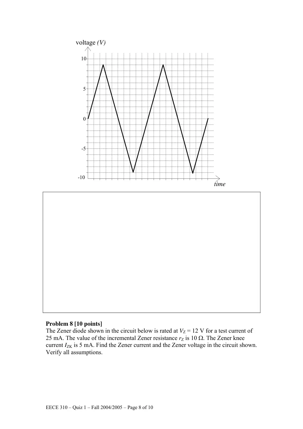
For the vS waveform shown below, plot and label, on the same graph, the output
waveform that is produced by the circuit shown above.
EECE 310 – Quiz 1 – Fall 2004/2005 – Page 8 of 10
time
voltage (V)
-5
0
5
10
-10
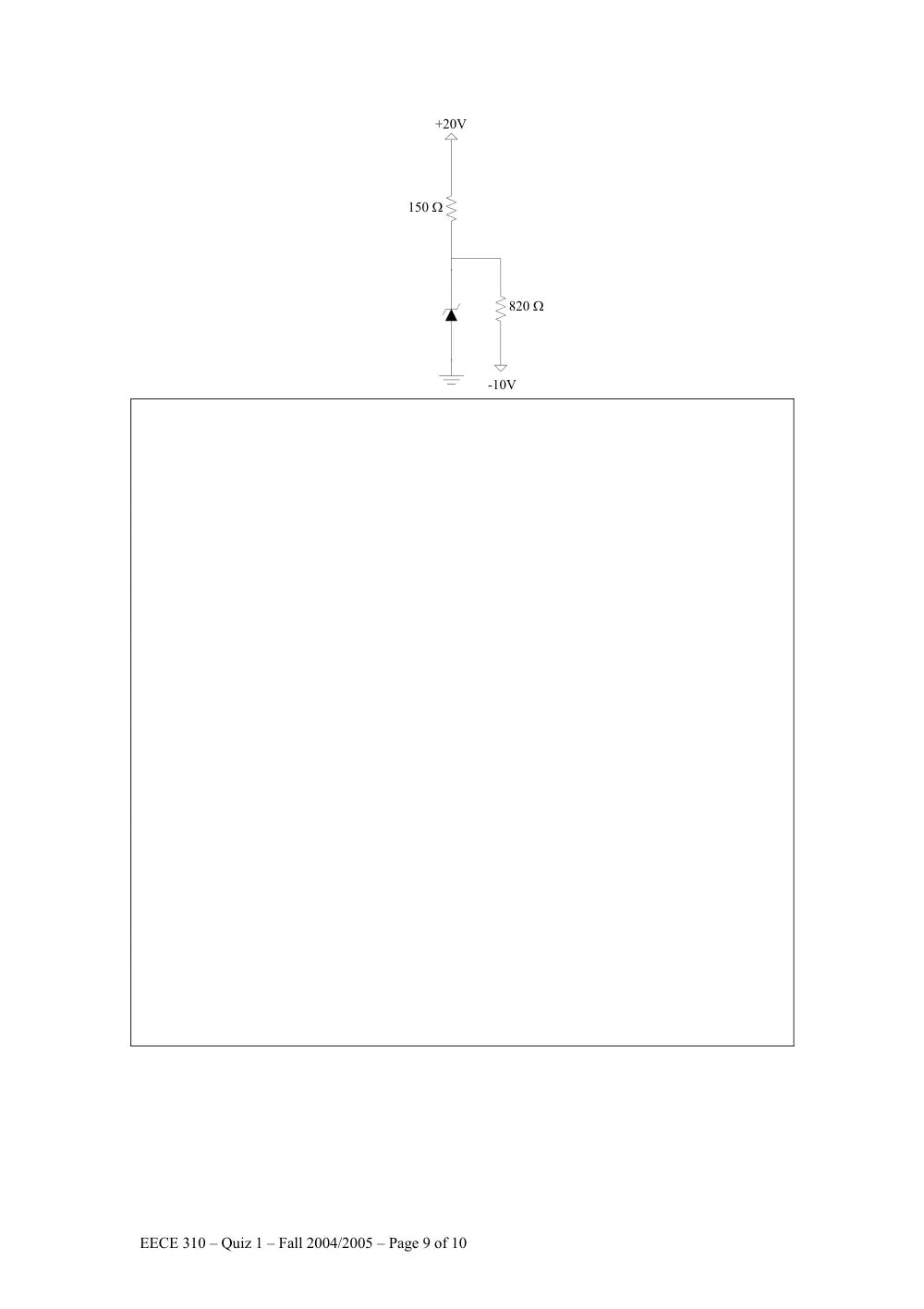
Problem 8 [10 points]
The Zener diode shown in the circuit below is rated at VZ = 12 V for a test current of
25 mA. The value of the incremental Zener resistance rZ is 10 Ω. The Zener knee
current IZK is 5 mA. Find the Zener current and the Zener voltage in the circuit shown.
Verify all assumptions.
EECE 310 – Quiz 1 – Fall 2004/2005 – Page 9 of 10
+20V
150 Ω
820 Ω
-10V
EECE 310 – Quiz 1 – Fall 2004/2005 – Page 10 of 10
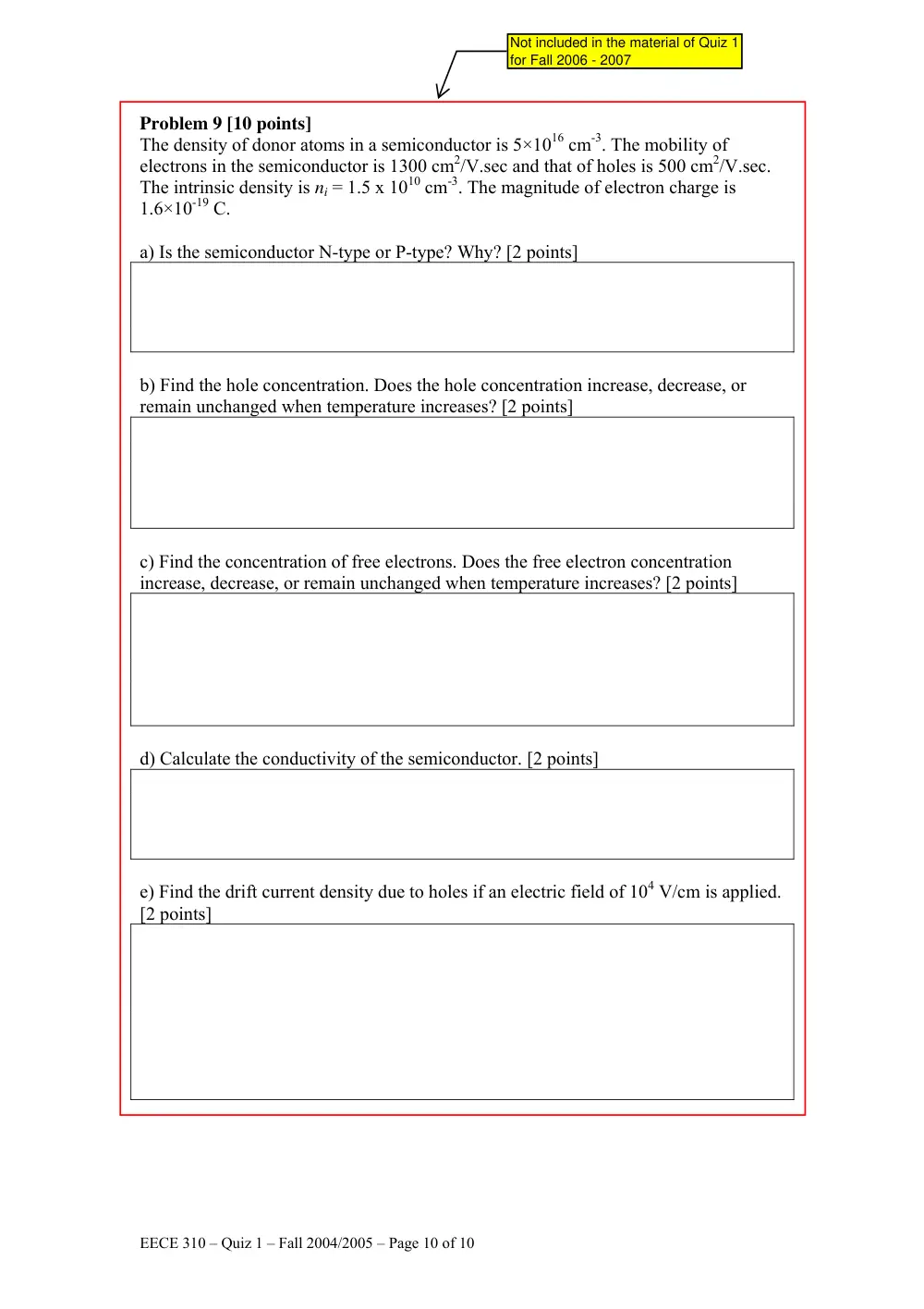
Problem 9 [10 points]
The density of donor atoms in a semiconductor is 5×1016 cm-3. The mobility of
electrons in the semiconductor is 1300 cm2/V.sec and that of holes is 500 cm2/V.sec.
The intrinsic density is ni = 1.5 x 1010 cm-3. The magnitude of electron charge is
1.6×10⁻¹⁹ C.
a) Is the semiconductor N-type or P-type? Why? [2 points]
b) Find the hole concentration. Does the hole concentration increase, decrease, or
remain unchanged when temperature increases? [2 points]
c) Find the concentration of free electrons. Does the free electron concentration
increase, decrease, or remain unchanged when temperature increases? [2 points]
d) Calculate the conductivity of the semiconductor. [2 points]
e) Find the drift current density due to holes if an electric field of 104 V/cm is applied.
[2 points]
Not included in the material of Quiz 1
for Fall 2006 - 2007