
EECE 310 Midterm, Fall 2012
American University of Beirut · Electronics · 7 pages
More EECE 310 files
- Midterm with Solutions · Fall 2014Exam · with solutionView
- Midterm · Fall 2014ExamView
- Midterm · Fall 2013ExamView
- Midterm with Solution · Summer 2011Exam · with solutionView
- Exam 2 with Answers · Fall 2011Exam · with solutionView
- Exam 1 with Answers · Fall 2011Exam · with solutionView
- Midterm · Summer 2010ExamView
- Exam 1 · Fall 2010ExamView
Show the text of this exam
EECE 310 – Midterm Exam – Fall 2012 - Page 1 of 7
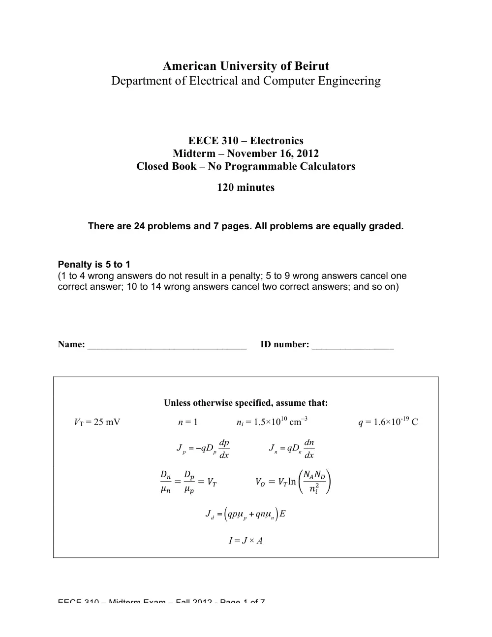
American University of Beirut
Department of Electrical and Computer Engineering
EECE 310 – Electronics
Midterm – November 16, 2012
Closed Book – No Programmable Calculators
120 minutes
There are 24 problems and 7 pages. All problems are equally graded.
Penalty is 5 to 1
(1 to 4 wrong answers do not result in a penalty; 5 to 9 wrong answers cancel one
correct answer; 10 to 14 wrong answers cancel two correct answers; and so on)
Name: _________________________________
ID number: _________________
Unless otherwise specified, assume that:
VT = 25 mV n = 1 ni = 1.5×1010 cm–3 q = 1.6×10⁻¹⁹ C
J p = −qDp
dp
dx J n = qDn
dn
dx
𝐷!
𝜇!
= 𝐷!
𝜇!
= 𝑉! 𝑉! = 𝑉!ln 𝑁!𝑁!
𝑛!
!
J d = qpµ p + qnµn
(
)E
I = J × A
EECE 310 – Midterm Exam – Fall 2012 - Page 2 of 7
1. A diode has a reverse saturation current Is = 10-12 A and n = 1.2. What is the diode forward
voltage drop (in mV) at a current of 4 mA?
a) 717.0
b) 704.9
c) 663.3
d) 684.1
e) 696.2
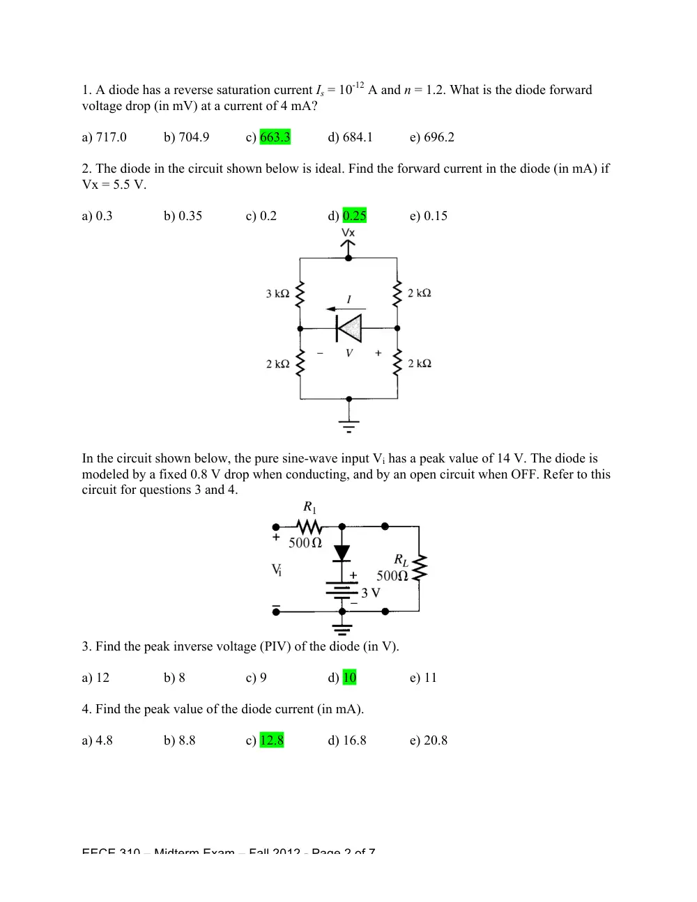
2. The diode in the circuit shown below is ideal. Find the forward current in the diode (in mA) if
Vx = 5.5 V.
a) 0.3
b) 0.35
c) 0.2
d) 0.25
e) 0.15
In the circuit shown below, the pure sine-wave input Vi has a peak value of 14 V. The diode is
modeled by a fixed 0.8 V drop when conducting, and by an open circuit when OFF. Refer to this
circuit for questions 3 and 4.
3. Find the peak inverse voltage (PIV) of the diode (in V).
a) 12
b) 8
c) 9
d) 10
e) 11
4. Find the peak value of the diode current (in mA).
a) 4.8
b) 8.8
c) 12.8
d) 16.8
e) 20.8
EECE 310 – Midterm Exam – Fall 2012 - Page 3 of 7
5. The average (DC) value of the output voltage of a half-wave rectifier is 6 V. If the diode is
ideal and the load is purely resistive, find the RMS value of the sinusoidal AC supply voltage (in
V rms) at the transformer secondary.
a) 31.1
b) 13.3
c) 17.8
d) 26.6
e) 22.2
6. A full-wave bridge rectifier with a filter capacitor is fed with a sinusoidal voltage source
vI = Vp × sin(2πft) V. The diode is ideal, the frequency f = 50 Hz, the capacitance C = 100 µF,
and the load resistance R = 50 kΩ. Find (Vr /Vp)×100, where Vr is the output ripple voltage.
a) 0.4
b) 0.5
c) 1
d) 0.2
e) 0.25
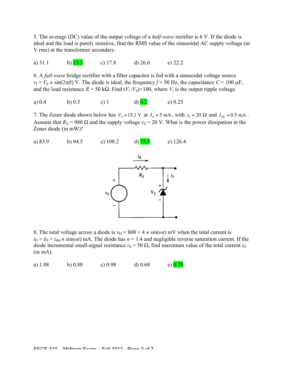
7. The Zener diode shown below has VZ =15.1 V at IZ = 5 mA , with rZ = 20 Ω and IZK = 0.5 mA .
Assume that RX = 980 Ω and the supply voltage vS = 20 V. What is the power dissipation in the
Zener diode (in mW)?
a) 83.9
b) 94.5
c) 108.2
d) 75.5
e) 126.4
8. The total voltage across a diode is vD = 800 + 4 × sin(ωt) mV when the total current is
iD = ID + idm × sin(ωt) mA. The diode has n = 1.4 and negligible reverse saturation current. If the
diode incremental small-signal resistance rd = 50 Ω, find maximum value of the total current iD
(in mA).
a) 1.08
b) 0.88
c) 0.98
d) 0.68
e) 0.78
EECE 310 – Midterm Exam – Fall 2012 - Page 4 of 7
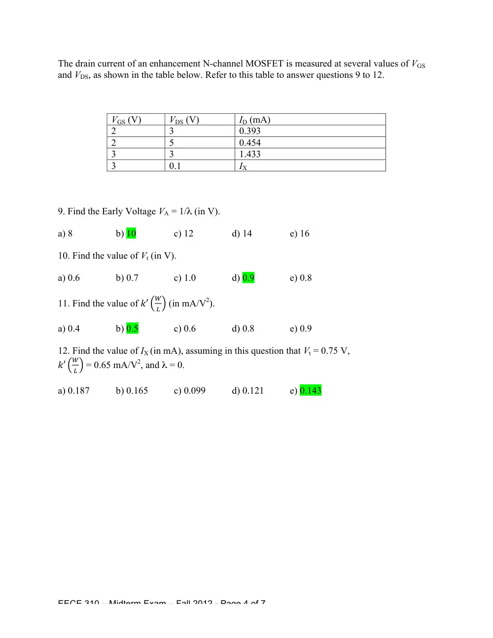
The drain current of an enhancement N-channel MOSFET is measured at several values of VGS
and VDS, as shown in the table below. Refer to this table to answer questions 9 to 12.
VGS (V)
VDS (V)
ID (mA)
2
3
0.393
2
5
0.454
3
3
1.433
3
0.1
IX
9. Find the Early Voltage VA = 1/λ (in V).
a) 8
b) 10
c) 12
d) 14
e) 16
10. Find the value of Vt (in V).
a) 0.6
b) 0.7
c) 1.0
d) 0.9
e) 0.8
11. Find the value of 𝑘′
!
! (in mA/V2).
a) 0.4
b) 0.5
c) 0.6
d) 0.8
e) 0.9
12. Find the value of IX (in mA), assuming in this question that Vt = 0.75 V,
𝑘′
!
! = 0.65 mA/V2, and λ = 0.
a) 0.187
b) 0.165
c) 0.099
d) 0.121
e) 0.143
EECE 310 – Midterm Exam – Fall 2012 - Page 5 of 7
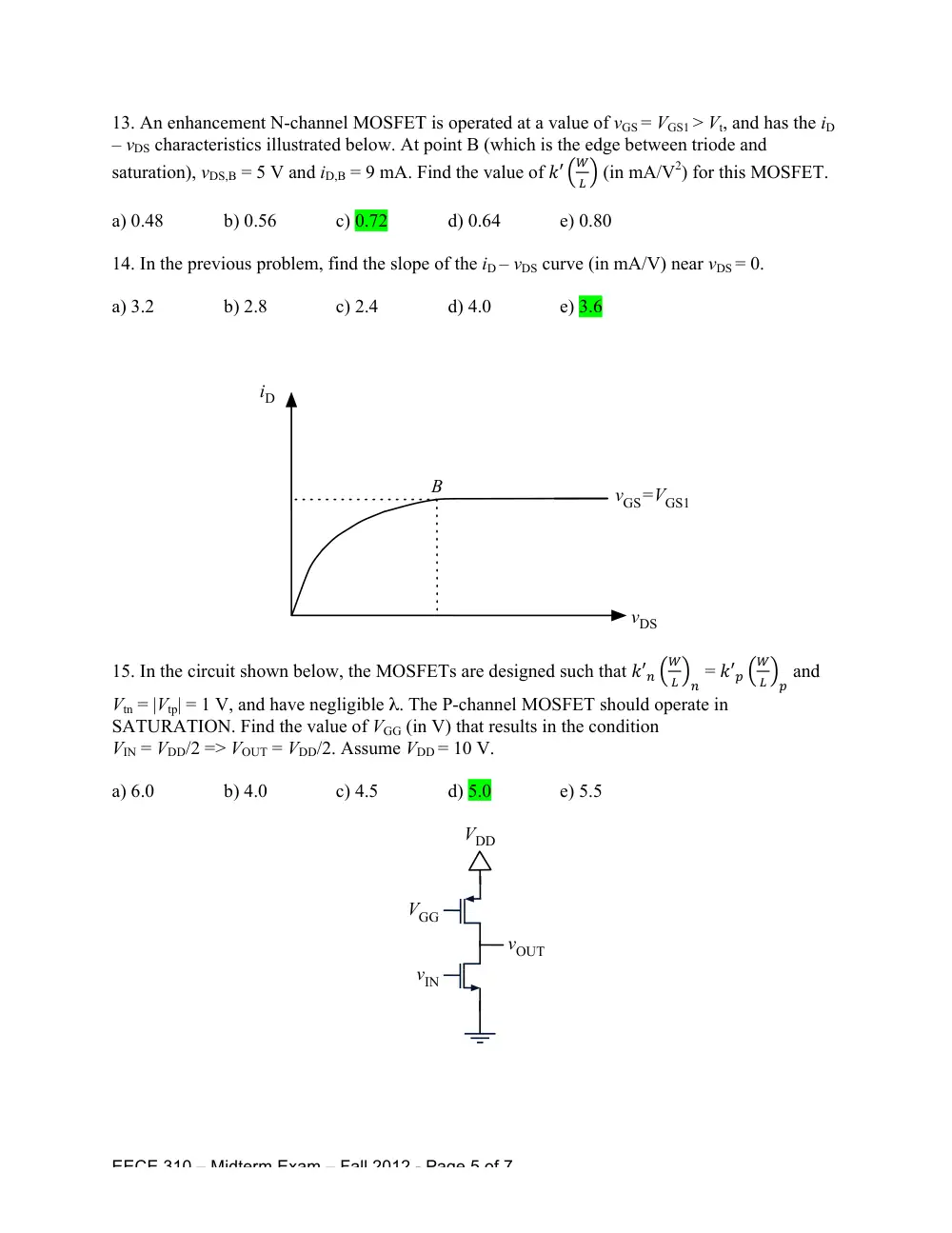
13. An enhancement N-channel MOSFET is operated at a value of vGS = VGS1 > Vt, and has the iD
– vDS characteristics illustrated below. At point B (which is the edge between triode and
saturation), vDS,B = 5 V and iD,B = 9 mA. Find the value of 𝑘′
!
! (in mA/V2) for this MOSFET.
a) 0.48
b) 0.56
c) 0.72
d) 0.64
e) 0.80
14. In the previous problem, find the slope of the iD – vDS curve (in mA/V) near vDS = 0.
a) 3.2
b) 2.8
c) 2.4
d) 4.0
e) 3.6
15. In the circuit shown below, the MOSFETs are designed such that 𝑘′!
!
!
! = 𝑘′!
!
!
! and
Vtn = |Vtp| = 1 V, and have negligible λ. The P-channel MOSFET should operate in
SATURATION. Find the value of VGG (in V) that results in the condition
VIN = VDD/2 => VOUT = VDD/2. Assume VDD = 10 V.
a) 6.0
b) 4.0
c) 4.5
d) 5.0
e) 5.5
iD
vDS
B
vGS=VGS1
VDD
VGG
vIN
vOUT
EECE 310 – Midterm Exam – Fall 2012 - Page 6 of 7
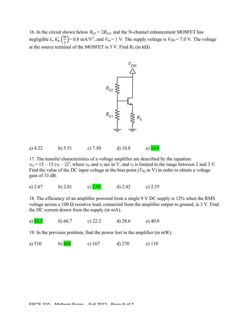
16. In the circuit shown below RG1 = 2RG2, and the N-channel enhancement MOSFET has
negligible λ, 𝑘!!
!
! = 0.8 mA/V2, and Vtn = 1 V. The supply voltage is VDD = 7.0 V. The voltage
at the source terminal of the MOSFET is 3 V. Find RS (in kΩ).
a) 4.22
b) 5.51
c) 7.50
d) 10.8
e) 16.9
17. The transfer characteristics of a voltage amplifier are described by the equation:
vO = 15 – 15 (vI – 2)4, where vO and vI are in V, and vI is limited to the range between 2 and 3 V.
Find the value of the DC input voltage at the bias point (VIQ in V) in order to obtain a voltage
gain of 33 dB.
a) 2.67
b) 2.81
c) 2.91
d) 2.42
e) 2.55
18. The efficiency of an amplifier powered from a single 9 V DC supply is 12% when the RMS
voltage across a 100 Ω resistive load, connected from the amplifier output to ground, is 3 V. Find
the DC current drawn from the supply (in mA).
a) 83.3
b) 66.7
c) 22.2
d) 28.6
e) 40.0
19. In the previous problem, find the power lost in the amplifier (in mW).
a) 510
b) 660
c) 167
d) 270
e) 110
RG2
RS
VDD
RG1
EECE 310 – Midterm Exam – Fall 2012 - Page 7 of 7
20. The transfer characteristics of a voltage amplifier are described by the following equation:
vO = 3 + 12vI with saturation levels at vO = –3 V and at vO = +4.2 V.
The input voltage vI = A + B sin(t) produces the largest undistorted output (i.e. largest D in
vO = C + D sin(t)). Find this maximum value of D (in V).
a) 3.60
b) 3.45
c) 3.30
d) 3.90
e) 3.75
21. In the previous problem, find the value of A (in V).
a) –0.175
b) –0.225
c) –0.213
d) –0.200
e) –0.188
22. A semiconductor volume with length L = 1 cm and cross-sectional area A = 1 cm2 carries a
current of 1 mA when a voltage V = 6.1 µV is applied across its length. Find the doping density
(in cm–3) in the semiconductor when the majority carriers are electrons with a mobility of 1330
cm2/V.s. Note that the electric field is E = V/L.
a) 1.5×10¹⁸
b) 1.1×10¹⁸
c) 7.7×10¹⁷
d) 5.2×10¹⁷
e) 4.7×10¹⁸
23. A doped semiconductor with a free electron density n(x) = a0 + a1 x, is also subjected to an
electric field E with intensity E(x) = 3VT a1/(a0 + a1 x), where VT is the thermal voltage. Find the
ratio of electron drift current density to electron diffusion current density
(Jdrift / Jdiffusion).
a) 4
b) 5
c) 6
d) 2
e) 3
24. The potential barrier across a PN junction doped such that NA = 2A ni, and ND = 3A ni, is
20VT. Find the value of A.
a) 14800
b) 24400
c) 40300
d) 66400
e) 9000