
EECE 310 Exam 1, Fall 2008
American University of Beirut · Electronics · 8 pages


More EECE 310 files
- Midterm with Solutions · Fall 2014Exam · with solutionView
- Midterm · Fall 2014ExamView
- Midterm · Fall 2013ExamView
- Midterm · Fall 2012ExamView
- Exam 2 with Answers · Fall 2011Exam · with solutionView
- Exam 1 with Answers · Fall 2011Exam · with solutionView
- Midterm with Solution · Summer 2011Exam · with solutionView
- Exam 1 · Fall 2010ExamView
Show the text of this exam
EECE 310 – Quiz 1 – Fall 2008-2009
Page 1 of 8
American University of Beirut
Department of Electrical and Computer Engineering
EECE 310 – Electronics
Quiz 1 – November 14, 2008
Closed Book – No Programmable Calculators
90 minutes
Penalty is 5 to 1
(1 to 4 wrong answers do not result in a penalty; 5 to 9 wrong answers cancel one
correct answer; 10 to 14 wrong answers cancel two correct answers; and so on)
Name: _____ANSWERS____________________________
ID number: _________________
Assume that VT = 25 mV, n = 1.5 (unless otherwise specified.)
p
p
dp
J
= −qD dx
n
n
dn
J
= qD dx
(
)
d
p
n
J
qp
qn
E
μ
μ
=
+
I = J × A
0
2
ln
A
D
T
i
N N
V
V
n
⎛
⎞
=
⎜
⎟
⎝
⎠
EECE 310 – Quiz 1 – Fall 2008-2009
Page 2 of 8
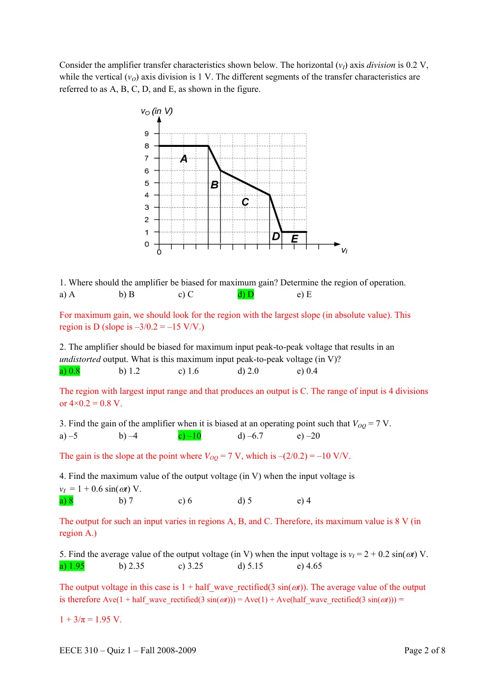
Consider the amplifier transfer characteristics shown below. The horizontal (vI) axis division is 0.2 V,
while the vertical (vO) axis division is 1 V. The different segments of the transfer characteristics are
referred to as A, B, C, D, and E, as shown in the figure.
1. Where should the amplifier be biased for maximum gain? Determine the region of operation.
a) A
b) B
c) C
d) D
e) E
For maximum gain, we should look for the region with the largest slope (in absolute value). This
region is D (slope is –3/0.2 = –15 V/V.)
2. The amplifier should be biased for maximum input peak-to-peak voltage that results in an
undistorted output. What is this maximum input peak-to-peak voltage (in V)?
a) 0.8
b) 1.2
c) 1.6
d) 2.0
e) 0.4
The region with largest input range and that produces an output is C. The range of input is 4 divisions
or 4×0.2 = 0.8 V.
3. Find the gain of the amplifier when it is biased at an operating point such that VOQ = 7 V.
a) –5
b) –4
c) –10
d) –6.7
e) –20
The gain is the slope at the point where VOQ = 7 V, which is –(2/0.2) = –10 V/V.
4. Find the maximum value of the output voltage (in V) when the input voltage is
vI = 1 + 0.6 sin(ωt) V.
a) 8
b) 7
c) 6
d) 5
e) 4
The output for such an input varies in regions A, B, and C. Therefore, its maximum value is 8 V (in
region A.)
5. Find the average value of the output voltage (in V) when the input voltage is vI = 2 + 0.2 sin(ωt) V.
a) 1.95
b) 2.35
c) 3.25
d) 5.15
e) 4.65
The output voltage in this case is 1 + half_wave_rectified(3 sin(ωt)). The average value of the output
is therefore Ave(1 + half_wave_rectified(3 sin(ωt))) = Ave(1) + Ave(half_wave_rectified(3 sin(ωt))) =
1 + 3/π = 1.95 V.
EECE 310 – Quiz 1 – Fall 2008-2009
Page 3 of 8
XXXXXXXXXXXXXXXXXXXXXXXXXXXXXXXXXXXXXXXXXXXXXXXXXXXXXXXX
6. If the gain of a voltage amplifier is 100, and its clipping levels at the output are +/– 10 V, what
should the peak value for an input sine voltage be (in V) in order to have the output voltage clipped at
35% of the RMS value of the input voltage?
a) 40.4
b) 47.14
c) 23.57
d) 17.68
e) 35.36
The output voltage is clipped at 10 V, which is 35% of the RMS value of the input voltage. For a sine
wave, the RMS value is the 0.7071×peak value. Therefore (35/100)×0.7071 VI_peak = 10, which gives
VI_peak = 40.4 V
XXXXXXXXXXXXXXXXXXXXXXXXXXXXXXXXXXXXXXXXXXXXXXXXXXXXXXXX
7. An amplifier is connected to +/– 5 V DC supplies from which it is drawing a current of 30 mA
(from each of the two supplies). The amplifier supplies a load of 75 Ω with an 4 V peak sine wave
while drawing a negligible current from a 0.8 V peak sine input signal. What is the efficiency of this
amplifier?
a) 26.67%
b)13.3%
c) 8.89% d) 35.6%
e) 21.3%
The power coming from the supplies is 5×30 + 5×30 = 300 mW. The output power in the load is
V2
O_peak /(2R) = 42/150 = 106.7 mW. The efficiency is therefore 106.7/300 × 100% = 35.6%
XXXXXXXXXXXXXXXXXXXXXXXXXXXXXXXXXXXXXXXXXXXXXXXXXXXXXXXX
8. The hole concentration in a p-type silicon sample is described by:
3
16
( )
10
10 exp(
/
p )
p x
x L
=
+
−
holes/cm3, where Lp = 1.6 µm and Dp = 10 cm2/sec.
What is the cross sectional area A of the sample (in μm2) if the diffusion current at x = Lp/2 is 100 μA?
a) 115.4
b) 271.8
c) 164.9
d) 139.6
e) 128.4
� � �
� �
�
����
��
��
�
�
� ��
�� 10����� ��
⁄
� ����� �
⁄
10�����
� 10�� � 1.6 � 10�� � 1.649
10�� � 1.6 � 10��� � 10��
� 164.9 � 10�� ��
XXXXXXXXXXXXXXXXXXXXXXXXXXXXXXXXXXXXXXXXXXXXXXXXXXXXXXXX
9. If the doping concentration of the p side in a PN junction is increased by 30%, find the incremental
change (in mV) for the built-in potential barrier.
a) 4.56
b) 6.56
c) 8.41
d) 10.13
e) 2.38
��� � ��� � �� ln �
�����
��
�
� � �� ln �
�����
��
�
� � �� ln �
���
���� � 25 ln�1.3� � 6.56 ��
XXXXXXXXXXXXXXXXXXXXXXXXXXXXXXXXXXXXXXXXXXXXXXXXXXXXXXXX
10. Which of the following statements is true?
a) Holes move in Silicon due to diffusion mechanism whereas free electrons move due to drift
EECE 310 – Quiz 1 – Fall 2008-2009
Page 4 of 8
mechanism
b) Drift is associated with the flow of holes from the region of high concentration to the region of low
concentration
c) Drift is associated with random motion due to thermal agitation
d) Diffusion occurs when an electric field is applied across a semiconductor
e) Free electrons drift in the direction opposite to that of the applied electric field
XXXXXXXXXXXXXXXXXXXXXXXXXXXXXXXXXXXXXXXXXXXXXXXXXXXXXXXX
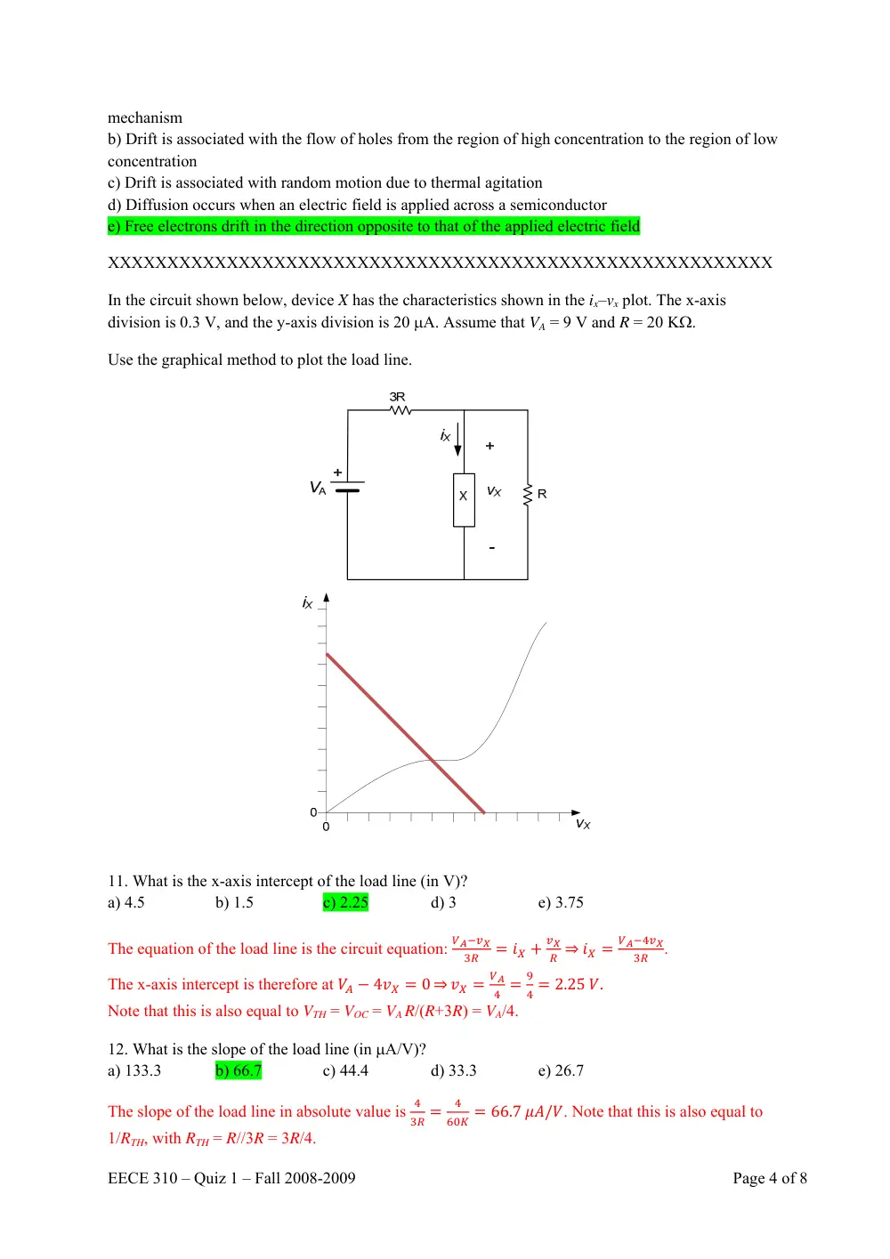
In the circuit shown below, device X has the characteristics shown in the ix–vx plot. The x-axis
division is 0.3 V, and the y-axis division is 20 μA. Assume that VA = 9 V and R = 20 KΩ.
Use the graphical method to plot the load line.
11. What is the x-axis intercept of the load line (in V)?
a) 4.5
b) 1.5
c) 2.25
d) 3
e) 3.75
The equation of the load line is the circuit equation:
�����
��
� �� �
��
� � �� �
������
��
.
The x-axis intercept is therefore at �� � 4�� � 0 � �� �
��
� �
�
� � 2.25 �.
Note that this is also equal to VTH = VOC = VA R/(R+3R) = VA/4.
12. What is the slope of the load line (in μA/V)?
a) 133.3
b) 66.7
c) 44.4
d) 33.3
e) 26.7
The slope of the load line in absolute value is
�
�� �
�
��� � 66.7 ��/�. Note that this is also equal to
1/RTH, with RTH = R//3R = 3R/4.
EECE 310 – Quiz 1 – Fall 2008-2009
Page 5 of 8
13. What is the bias point voltage (VX) of the device (in V)?
a) 0.88
b) 1.35
c) 1.88
d) 3.36
e) 2.5
The x-axis intercept is 2.25 V, which is 2.25/0.3 = 7.5 divisions.
The y-axis intercept is
��
�� �
�
��� � 150��, which corresponds to 7.5 divisions.
The plot shows the load line. The bias point is at (4.5 to 5) x-axis divisions, or around 1.35 V (closest
answer.)
XXXXXXXXXXXXXXXXXXXXXXXXXXXXXXXXXXXXXXXXXXXXXXXXXXXXXXXX
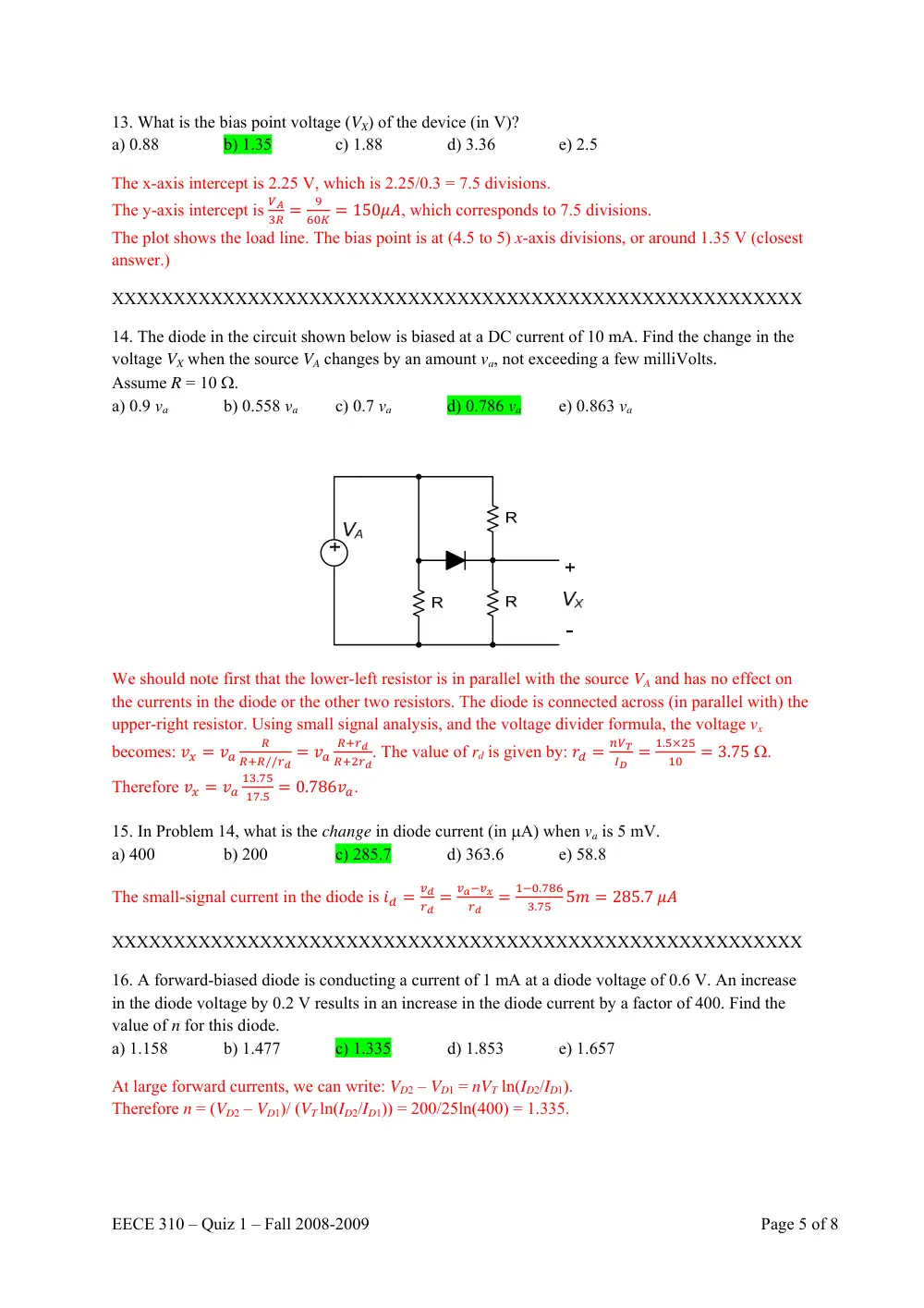
14. The diode in the circuit shown below is biased at a DC current of 10 mA. Find the change in the
voltage VX when the source VA changes by an amount va, not exceeding a few milliVolts.
Assume R = 10 Ω.
a) 0.9 va
b) 0.558 va
c) 0.7 va
d) 0.786 va
e) 0.863 va
We should note first that the lower-left resistor is in parallel with the source VA and has no effect on
the currents in the diode or the other two resistors. The diode is connected across (in parallel with) the
upper-right resistor. Using small signal analysis, and the voltage divider formula, the voltage vx
becomes: �� � ��
�
���//�� � ��
����
�����. The value of rd is given by: �� �
���
�� �
�.����
��
� 3.75 Ω.
Therefore �� � ��
��.��
��.� � 0.786��.
15. In Problem 14, what is the change in diode current (in μA) when va is 5 mV.
a) 400
b) 200
c) 285.7
d) 363.6
e) 58.8
The small-signal current in the diode is �� �
��
�� �
�����
��
�
���.���
�.��
5� � 285.7 ��
XXXXXXXXXXXXXXXXXXXXXXXXXXXXXXXXXXXXXXXXXXXXXXXXXXXXXXXX
16. A forward-biased diode is conducting a current of 1 mA at a diode voltage of 0.6 V. An increase
in the diode voltage by 0.2 V results in an increase in the diode current by a factor of 400. Find the
value of n for this diode.
a) 1.158
b) 1.477
c) 1.335
d) 1.853
e) 1.657
At large forward currents, we can write: VD2 – VD1 = nVT ln(ID2/ID1).
Therefore n = (VD2 – VD1)/ (VT ln(ID2/ID1)) = 200/25ln(400) = 1.335.
EECE 310 – Quiz 1 – Fall 2008-2009
Page 6 of 8
17. The same diode of Problem 16 is now connected in series with a 27 MΩ resistor and a 5 V battery,
such that the diode is reverse biased. Find the voltage across the 27 MΩ resistor (in mV).
a) 27×10–3
b) 0.422
c) 64
d) 13.8
e) 2.37
The diode is reverse biased, with a reverse bias of a few Volts. We can therefore safely assume that
the current in the diode is equal to –IS. The value of IS is calculated from the given of Problem 16:
�� � 1� � �� �exp �
�.�
�.�������� � 1� � �� � 15.6 ��.The drop across the resistor is RIS = 0.422 mV.
XXXXXXXXXXXXXXXXXXXXXXXXXXXXXXXXXXXXXXXXXXXXXXXXXXXXXXXX
18. A Zener diode is connected as shown in the circuit below. Find the power dissipation in the Zener
diode (in mW). Assume that VA = 10 V, R1 = 220 Ω, R2 = 330 Ω, VZ0 = 5.4, rZ = 10 Ω, IZK = 2 mA, and
IZMAX = 200 mA.
a) 32.7
b) 23.0
c) 59.9
d) 52.9
e) 43.9
The Zener voltage is given by �� � �
��
�� �
���
�� � ���//��//��� = 5.442 V. The Zener current is IZ =
(VZ – VZ0)/rZ = 4.23 mA (between IZK and IZMAX). The power dissipation in the Zener is IZVZ = 23 mW.
19. Find the voltage (in V) across the Zener when R2 = 120 Ω.
a) 3.5
b) 4.5
c) 4.3
d) 4.7
e) 5.5
The Zener voltage in this case is given by �� � �
��
�� �
���
�� � ���//��//��� = 5.19 V. This however is
smaller than VZ0. Therefore, the Zener is not in the breakdown region: it is not conducting any
(sizeable) current. The Zener is OFF and the voltage across the Zener is given by the voltage divider
formula: VZ = VA R2 / (R1 + R2) = 3.5 V.
XXXXXXXXXXXXXXXXXXXXXXXXXXXXXXXXXXXXXXXXXXXXXXXXXXXXXXXX
20. The input to a half-wave rectifier is a square wave with zero average, a peak value of 7 V, and
frequency of 100 Hz. The diode drops 0.7 V when conducting. The load is a 3 KΩ resistor. Find the
average value of the load current (in the resistor; in mA).
a) 1.55
b) 0.88
c) 1.05
d) 1.22
e) 1.38
EECE 310 – Quiz 1 – Fall 2008-2009
Page 7 of 8
The load current is a half-wave-rectified square wave (positive parts only), with a pulse (or peak)
level of (7 – 0.7) / 3K = 2.1 mA. The average value of such a square wave is one half the pulse level
or 2.1/2 = 1.05 mA.
21. A 330 μF capacitor is now connected in parallel with the load, in the circuit of Problem 20. Find
the value of the resulting ripple voltage (in mV).
a) 20.3
b) 15.5
c) 40
d) 31.7
e) 25.8
The diode discharges during half the cycle (see figure above):
VRIPPLE = VO_PEAK – VO_PEAK exp(–(T/2) / (RC) ) =
(7 – 0.7) × (1 – exp(–1/(2×100×3000×330×10–6))) = 31.7 mV
22. Find the PIV (in V) of the diode in the circuit of Problem 21.
a) 19.3
b) 11.3
c) 13.3
d) 15.3
e) 17.3
The most negative voltage on the diode occurs when the input switches from +Vmax to –Vmax. The
absolute value of the diode voltage in this case is 2Vmax – VD = 14 – 0.7 = 13.3 V.
XXXXXXXXXXXXXXXXXXXXXXXXXXXXXXXXXXXXXXXXXXXXXXXXXXXXXXXX
In the circuit shown below, assume VA = 5 V, VB = 15 V, and R = 1 KΩ. The diodes are ideal.
23. Find the value of the input voltage (in V) at which diode D1 starts to conduct.
a) 6
b) 4
c) 3
d) 2
e) 5
D1 starts to conduct when Vi becomes equal to VA = 5 V.
EECE 310 – Quiz 1 – Fall 2008-2009
Page 8 of 8
24. Find the peak-to-peak variation in the output voltage (in V) when the input voltage is
vI = –20 + 1.5 sin(ωt) V.
a) 2
b) 1.6
c) 2.4
d) 1.2
e) 0.8
The input voltage varies between –20 – 1.5 = –21.5 V to –20 + 1.5 = –18.5 V. For this range of
voltages, diode D2 is ON, while diode D1 is OFF. The current in D2 is ID2 = (–Vi – VB) / (R + 2R).
The output voltage is –VB – 2R×ID2 = –VB + 2(Vi + VB)/3
Since VB is a DC voltage, the time-varying component in the output voltage has a peak-to-peak value
equal to 2Vi_peak-to-peak / 3 = 2×2×1.5 /3 = 2 V.
XXXXXXXXXXXXXXXXXXXXXXXXXXXXXXXXXXXXXXXXXXXXXXXXXXXXXXXX
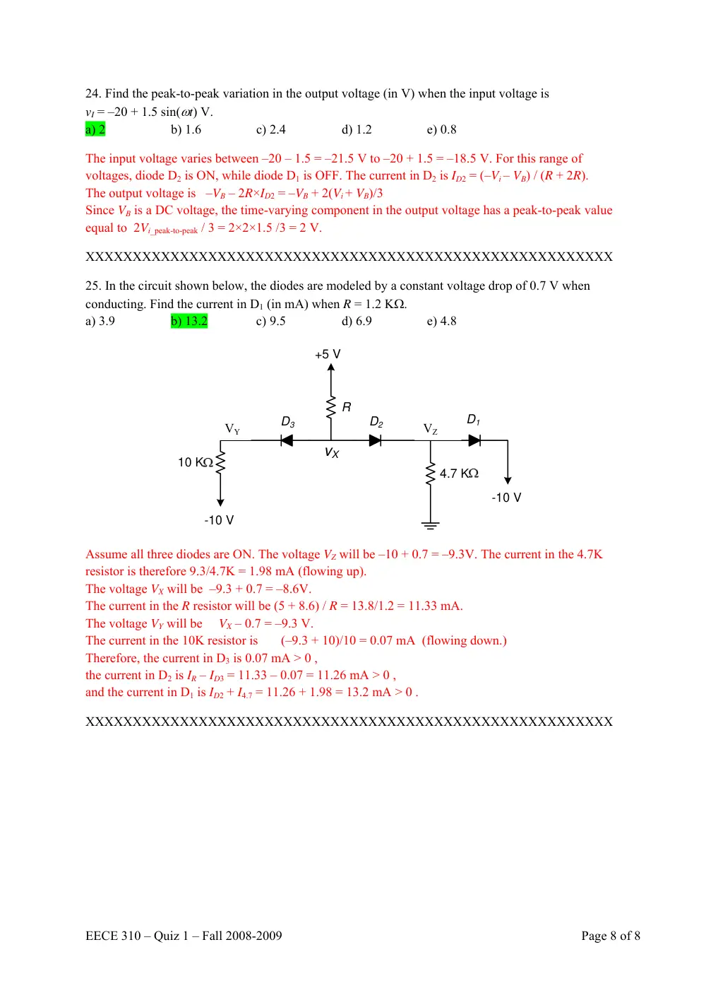
25. In the circuit shown below, the diodes are modeled by a constant voltage drop of 0.7 V when
conducting. Find the current in D1 (in mA) when R = 1.2 KΩ.
a) 3.9
b) 13.2
c) 9.5
d) 6.9
e) 4.8
vX
R
4.7 K
10 K
-10 V
-10 V
+5 V
D1
D2
D3
Assume all three diodes are ON. The voltage VZ will be –10 + 0.7 = –9.3V. The current in the 4.7K
resistor is therefore 9.3/4.7K = 1.98 mA (flowing up).
The voltage VX will be –9.3 + 0.7 = –8.6V.
The current in the R resistor will be (5 + 8.6) / R = 13.8/1.2 = 11.33 mA.
The voltage VY will be VX – 0.7 = –9.3 V.
The current in the 10K resistor is (–9.3 + 10)/10 = 0.07 mA (flowing down.)
Therefore, the current in D3 is 0.07 mA > 0 ,
the current in D2 is IR – ID3 = 11.33 – 0.07 = 11.26 mA > 0 ,
and the current in D1 is ID2 + I4.7 = 11.26 + 1.98 = 13.2 mA > 0 .
XXXXXXXXXXXXXXXXXXXXXXXXXXXXXXXXXXXXXXXXXXXXXXXXXXXXXXXX
VY
VZ