
EECE 310 Exam 2, Fall 2006
American University of Beirut · Electronics · 7 pages

More EECE 310 files
- Midterm · Fall 2014ExamView
- Midterm with Solutions · Fall 2014Exam · with solutionView
- Midterm · Fall 2013ExamView
- Midterm · Fall 2012ExamView
- Midterm with Solution · Summer 2011Exam · with solutionView
- Exam 2 with Answers · Fall 2011Exam · with solutionView
- Exam 1 with Answers · Fall 2011Exam · with solutionView
- Exam 1 · Fall 2010ExamView
Show the text of this exam
EECE 310 – Electronics I – Quiz 2 – Fall 2006-2007 - Page 1 of 7
American University of Beirut
Department of Electrical and Computer Engineering
EECE 310 – Electronics I
Quiz 2 – December 16, 2006
Closed Book – No Programmable Calculators
120 minutes
Penalty is 5 to 1
Name: _________________________________
ID number: _________________
Use
ni ≈ 1.25×10¹⁰ / cm3
Dp = 12 cm2/s, Dn= 34 cm2/s
μp = 480 cm2/V.s, μn = 1350 cm2/V.s.
q = 1.6×10⁻¹⁹ C, VT ≈ 25 mV, εSi = 1.04 × 10⁻¹² F/cm
1 μm = 10-4 cm
1 fF = 10-15 F
Neglect body effect
▬▬▬▬▬▬▬▬
1- A MOSFET is biased in the saturation region at a fixed VDS, and at ID = 2 mA, and
VOV = 1 V. Find the increase in the drain current (in mA) when the gate-to-source
voltage increases by 10 mV.
a) 0.08
b) 0.07
c) 0.04
d) 0.05
e) 0.06
▬▬▬▬▬▬▬▬
2- A MOSFET with k’n(W/L) = 1 mA/V2, Vt = 1.3 V, and λ = 0.04 V–1, is biased at
VGS = 2 V, VDS = 4 V. Find the value of ro (in KΩ) for this MOSFET.
a) 88.9
b) 102.0
c) 61.7
d) 69.2
e) 78.1
▬▬▬▬▬▬▬▬
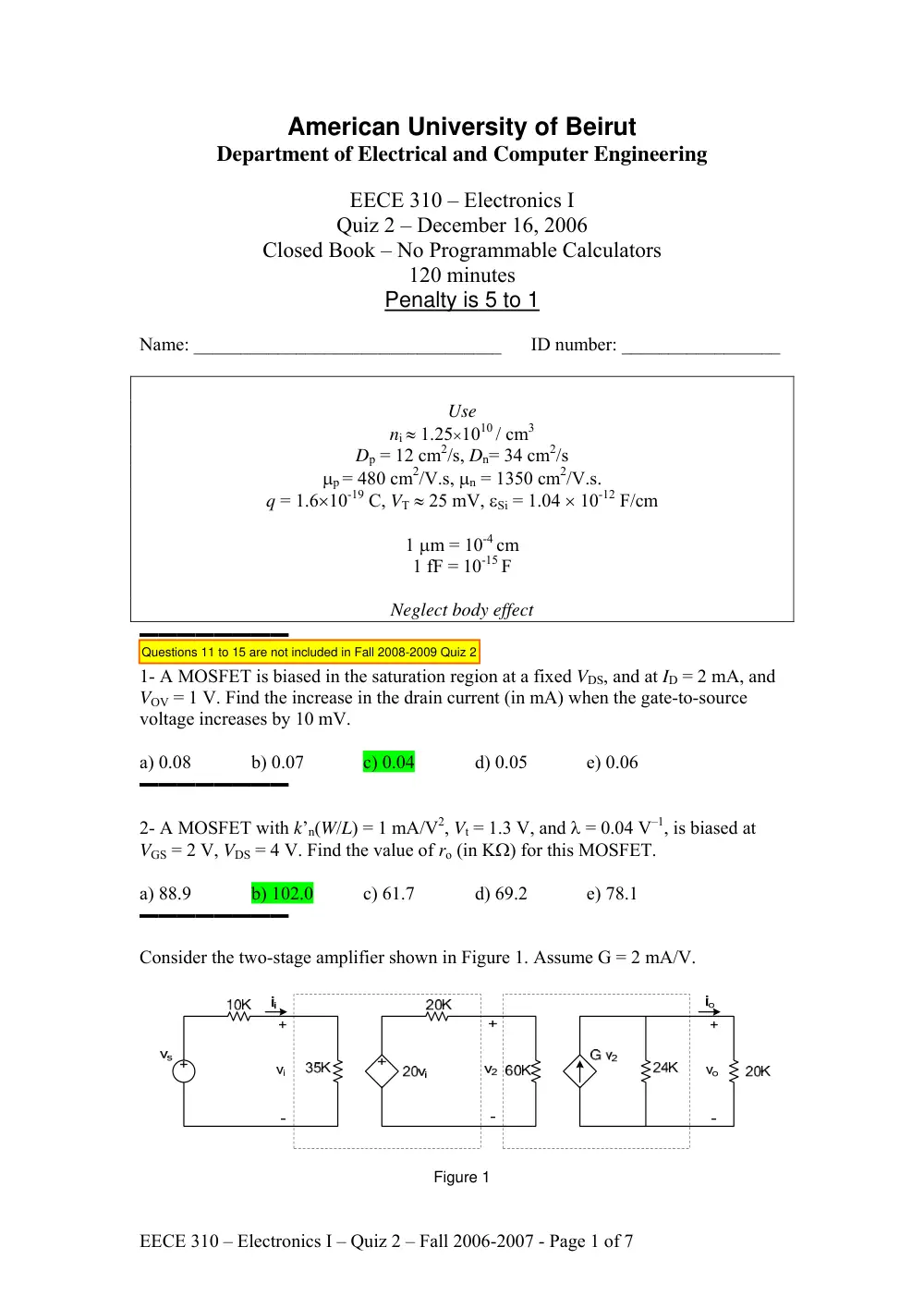
Consider the two-stage amplifier shown in Figure 1. Assume G = 2 mA/V.
Figure 1
Questions 11 to 15 are not included in Fall 2008-2009 Quiz 2
EECE 310 – Electronics I – Quiz 2 – Fall 2006-2007 - Page 2 of 7
3- Find the value of the input resistance (in KΩ).
a) 30
b) 35
c) 40
d) 45
e) 50
4- Find the value of the output resistance (in KΩ).
a) 15
b) 27
c) 24
d) 21
e) 18
5- Find the voltage gain of the amplifier (vo/vi).
a) 257.1
b) 307.3
c) 284.2
d) 344.7
e) 327.3
6- Find the current gain (io/ii).
a) 517.0
b) 572.7
c) 614.6
d) 639.5
e) 642.9
▬▬▬▬▬▬▬▬
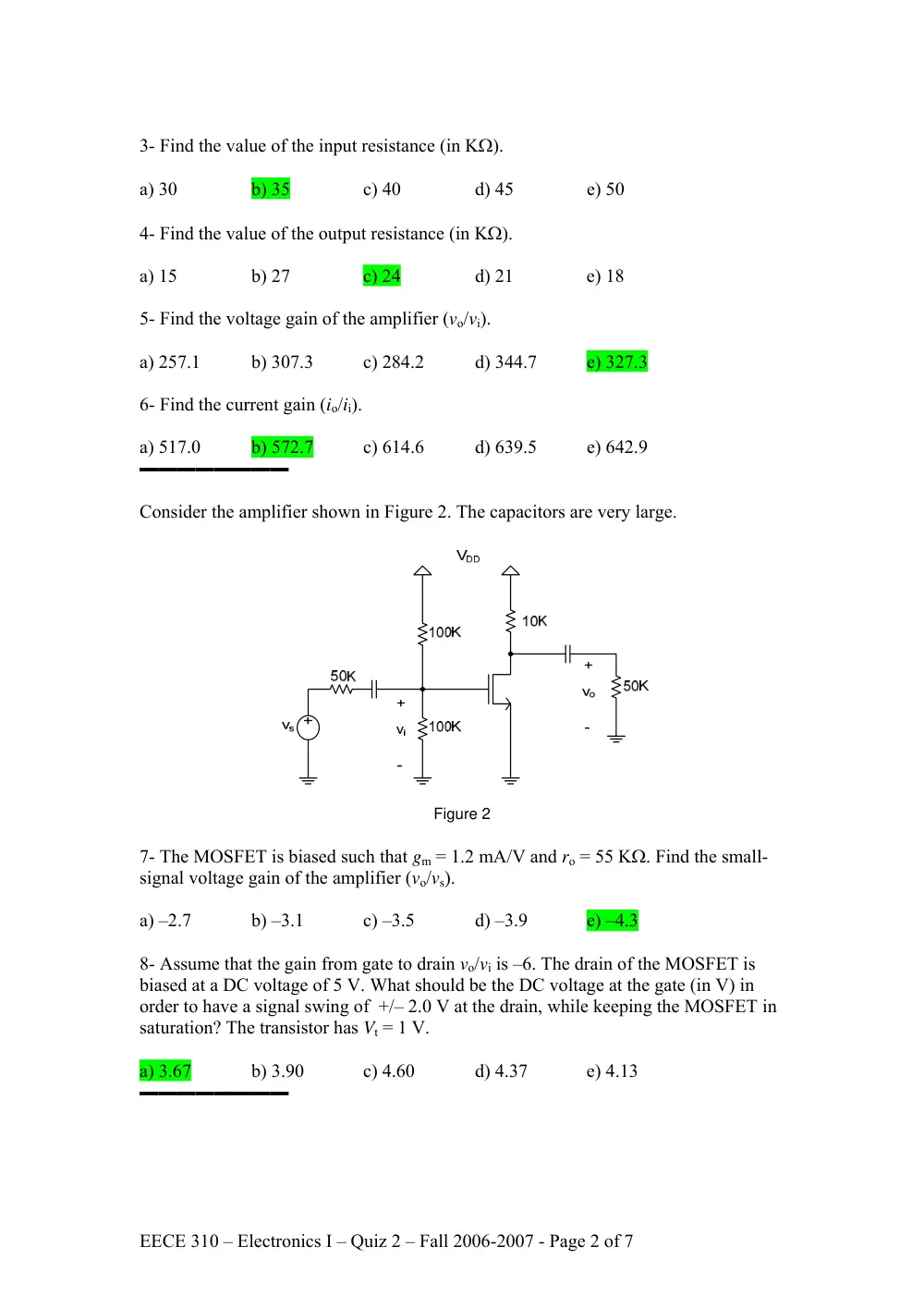
Consider the amplifier shown in Figure 2. The capacitors are very large.
Figure 2
7- The MOSFET is biased such that gm = 1.2 mA/V and ro = 55 KΩ. Find the small-
signal voltage gain of the amplifier (vo/vs).
a) –2.7
b) –3.1
c) –3.5
d) –3.9
e) –4.3
8- Assume that the gain from gate to drain vo/vi is –6. The drain of the MOSFET is
biased at a DC voltage of 5 V. What should be the DC voltage at the gate (in V) in
order to have a signal swing of +/– 2.0 V at the drain, while keeping the MOSFET in
saturation? The transistor has Vt = 1 V.
a) 3.67
b) 3.90
c) 4.60
d) 4.37
e) 4.13
▬▬▬▬▬▬▬▬
EECE 310 – Electronics I – Quiz 2 – Fall 2006-2007 - Page 3 of 7
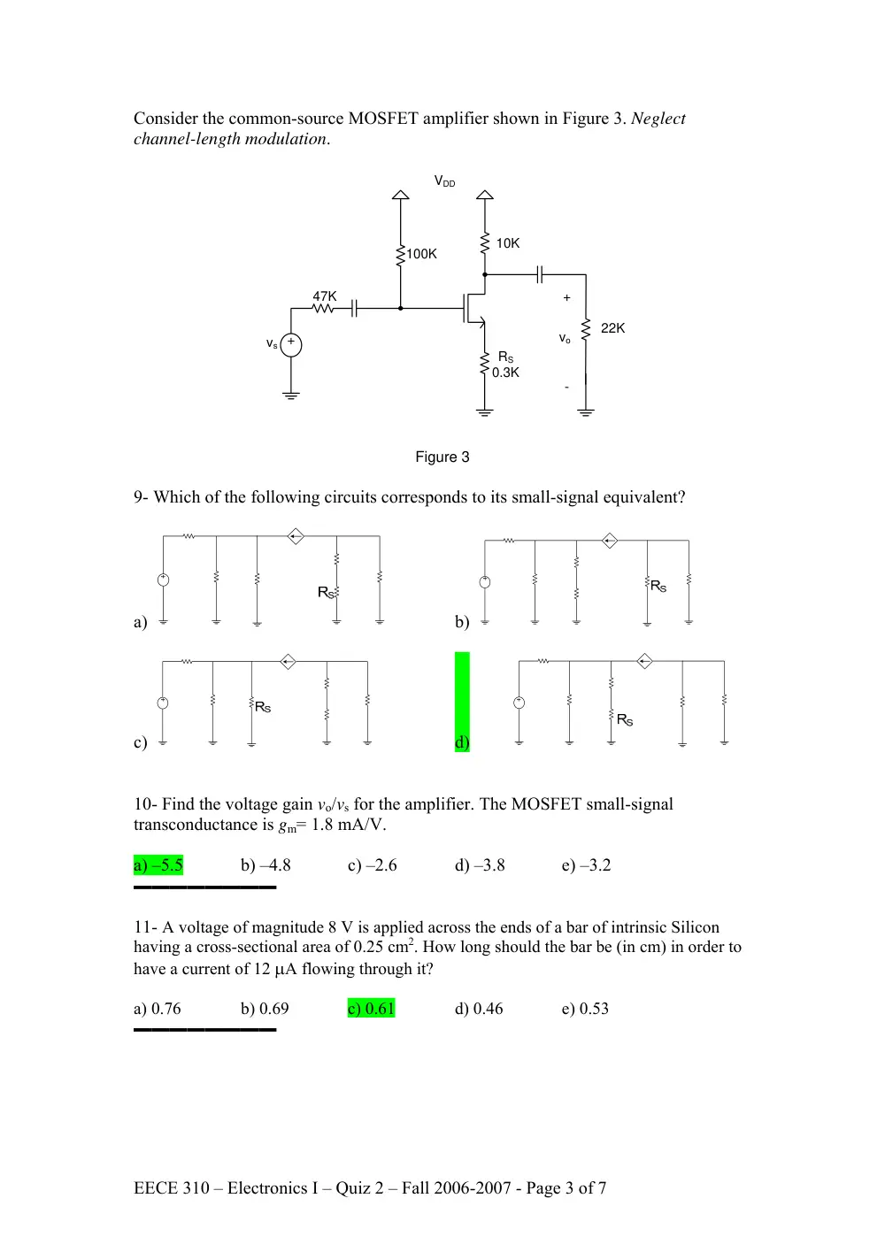
Consider the common-source MOSFET amplifier shown in Figure 3. Neglect
channel-length modulation.
vs +
vo
+
-
VDD
10K
100K
47K
22K
RS
0.3K
Figure 3
9- Which of the following circuits corresponds to its small-signal equivalent?
a)
b)
c)
d)
10- Find the voltage gain vo/vs for the amplifier. The MOSFET small-signal
transconductance is gm= 1.8 mA/V.
a) –5.5
b) –4.8
c) –2.6
d) –3.8
e) –3.2
▬▬▬▬▬▬▬▬
11- A voltage of magnitude 8 V is applied across the ends of a bar of intrinsic Silicon
having a cross-sectional area of 0.25 cm2. How long should the bar be (in cm) in order to
have a current of 12 μA flowing through it?
a) 0.76
b) 0.69
c) 0.61
d) 0.46
e) 0.53
▬▬▬▬▬▬▬▬
EECE 310 – Electronics I – Quiz 2 – Fall 2006-2007 - Page 4 of 7
For a particular PN junction, the acceptor concentration is 5×10¹⁶/cm3, and the donor
concentration is 3×10¹² /cm3.
12- Find the junction potential (in V) if no external bias is applied.
a) 0.46
b) 0.69
c) 0.63
d) 0.57
e) 0.52
13- Find the concentration of holes (in cm-3) in the n-type material.
a) 5.2×10⁶ b) 5.2×10⁸
c) 5.2×10⁷ d) 5.2×10⁴ e) 5.2×10⁵
14- Find the depletion capacitance (in fF) when an 8 V reverse-bias is applied across
this diode. The junction cross-sectional area is 500 µm2. The width of the depletion
region is given by
(
)
Si
o
R
A
D
2ε
1
1
W
V
V
q
N
N
⎛
⎞
=
+
+
⎜
⎟
⎝
⎠
.
a) 26
b) 8.5
c) 2.7
d) 0.86
e) 0.27
▬▬▬▬▬▬▬▬
15- The hole concentration in the n-type material of a PN junction diode under
forward bias is described by:
/ p
5
17
( )
10
10
x L
p x
e
−
=
+
holes/cm3
with Lp = 3 μm. Given that the cross-sectional area of the junction is 240 μm2, find the
hole diffusion current (in mA) that flows in the n-material at x = 2 μm.
a) 0.26
b) 0.39
c) 0.53
d) 0.66
e) 0.79
▬▬▬▬▬▬▬▬
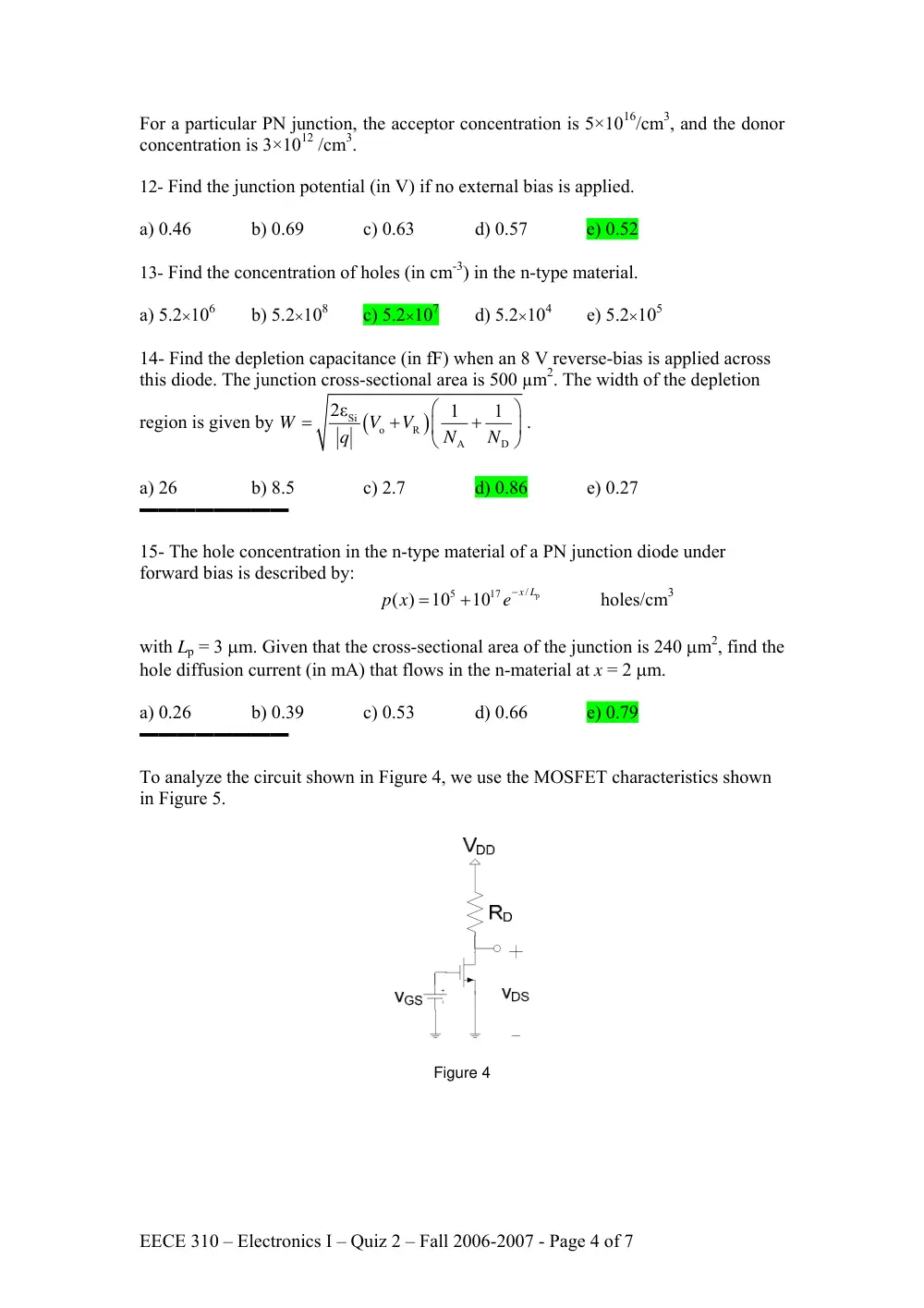
To analyze the circuit shown in Figure 4, we use the MOSFET characteristics shown
in Figure 5.
Figure 4
EECE 310 – Electronics I – Quiz 2 – Fall 2006-2007 - Page 5 of 7
2
4
6
8
10
vDS V
2
4
6
8
10
12
iD mA
A
B
C
vGS =2V
vGS =3V
vGS =4V
vGS =5V
Figure 5
Figure 5 shows the characteristics for an NMOS transistor for a set of values of VGS.
The lowest value of VGS is 1.5 V, the highest value is 10 V, with a step size of 0.5 V.
Also a load line for the resistor RD in the drain branch is shown in the figure. The
values for iD at the three points A, B, and C shown on the graph are:
iD(A) = 9.28 mA
iD(B) = 10.56 mA
iD(C) = 5.94 mA
16- What is the value of the resistor RD in Ω?
a) 1000
b) 800
c) 750
d) 1100
e) 1200
17- What is the value of VA in V? Use points A and B on the graph. Hint: Use the
MOSFET current equation in saturation.
a) 10
b) 25
c) 30
d) 20
e) 15
18- What is the value of Vt in V? Use points B and C on the graph. Hint: Use the
MOSFET current equation in saturation.
a) 1.0
b) 0.9
c) 0.8
d) 0.7
e) 0.6
EECE 310 – Electronics I – Quiz 2 – Fall 2006-2007 - Page 6 of 7
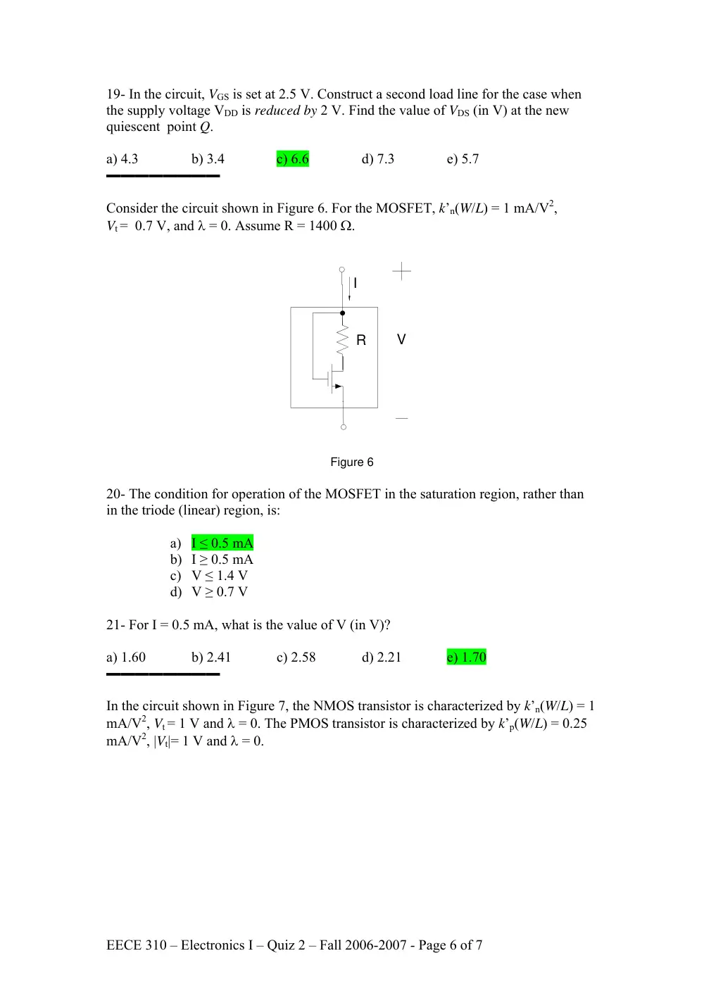
19- In the circuit, VGS is set at 2.5 V. Construct a second load line for the case when
the supply voltage VDD is reduced by 2 V. Find the value of VDS (in V) at the new
quiescent point Q.
a) 4.3
b) 3.4
c) 6.6
d) 7.3
e) 5.7
▬▬▬▬▬▬▬▬
Consider the circuit shown in Figure 6. For the MOSFET, k’n(W/L) = 1 mA/V2,
Vt = 0.7 V, and λ = 0. Assume R = 1400 Ω.
R
V
I
Figure 6
20- The condition for operation of the MOSFET in the saturation region, rather than
in the triode (linear) region, is:
a) I ≤ 0.5 mA
b) I ≥ 0.5 mA
c) V ≤ 1.4 V
d) V ≥ 0.7 V
21- For I = 0.5 mA, what is the value of V (in V)?
a) 1.60
b) 2.41
c) 2.58
d) 2.21
e) 1.70
▬▬▬▬▬▬▬▬
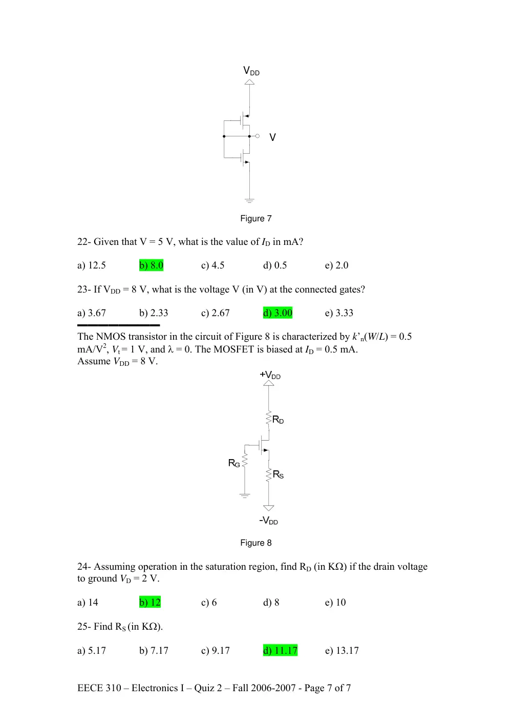
In the circuit shown in Figure 7, the NMOS transistor is characterized by k’n(W/L) = 1
mA/V2, Vt = 1 V and λ = 0. The PMOS transistor is characterized by k’p(W/L) = 0.25
mA/V2, |Vt|= 1 V and λ = 0.
EECE 310 – Electronics I – Quiz 2 – Fall 2006-2007 - Page 7 of 7
V
VDD
Figure 7
22- Given that V = 5 V, what is the value of ID in mA?
a) 12.5
b) 8.0
c) 4.5
d) 0.5
e) 2.0
23- If VDD = 8 V, what is the voltage V (in V) at the connected gates?
a) 3.67
b) 2.33
c) 2.67
d) 3.00
e) 3.33
▬▬▬▬▬▬▬▬
The NMOS transistor in the circuit of Figure 8 is characterized by k’n(W/L) = 0.5
mA/V2, Vt = 1 V, and λ = 0. The MOSFET is biased at ID = 0.5 mA.
Assume VDD = 8 V.
Figure 8
24- Assuming operation in the saturation region, find RD (in KΩ) if the drain voltage
to ground VD = 2 V.
a) 14
b) 12
c) 6
d) 8
e) 10
25- Find RS (in KΩ).
a) 5.17
b) 7.17
c) 9.17
d) 11.17
e) 13.17