
EECE 310 Exam 2, Fall 2007
American University of Beirut · Electronics · 6 pages


More EECE 310 files
- Midterm · Fall 2014ExamView
- Midterm with Solutions · Fall 2014Exam · with solutionView
- Midterm · Fall 2013ExamView
- Midterm · Fall 2012ExamView
- Midterm with Solution · Summer 2011Exam · with solutionView
- Exam 2 with Answers · Fall 2011Exam · with solutionView
- Exam 1 with Answers · Fall 2011Exam · with solutionView
- Exam 1 · Fall 2010ExamView
Show the text of this exam
EECE 310 – Electronics – Quiz 2 – Fall 2007-2008 - Page 1 of 6
American University of Beirut
Department of Electrical and Computer Engineering
EECE 310 – Electronics
Quiz 2 – December 7, 2007
Closed Book – No Programmable Calculators
90 minutes
Penalty is 5 to 1
Name: _________________________________
ID number: _________________
Use
ni ≈ 1.25×10¹⁰ / cm3
Dp = 12 cm2/s, Dn= 34 cm2/s
μp = 470 cm2/V.s, μn = 1333 cm2/V.s.
q = 1.6×10⁻¹⁹ C
k = 1.38×10⁻²³ J/K
1 μm = 10-4 cm
VT ≈ 25 mV (when T is not specified)
▬▬▬▬▬▬▬▬
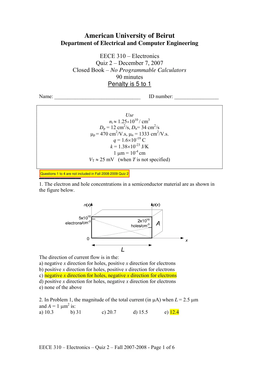
1. The electron and hole concentrations in a semiconductor material are as shown in
the figure below.
The direction of current flow is in the:
a) negative x direction for holes, positive x direction for electrons
b) positive x direction for holes, positive x direction for electrons
c) negative x direction for holes, negative x direction for electrons
d) positive x direction for holes, negative x direction for electrons
e) none of the above
2. In Problem 1, the magnitude of the total current (in μA) when L = 2.5 μm
and A = 1 μm2 is:
a) 10.3
b) 31
c) 20.7
d) 15.5
e) 12.4
Questions 1 to 4 are not included in Fall 2008-2009 Quiz 2
EECE 310 – Electronics – Quiz 2 – Fall 2007-2008 - Page 2 of 6
▬▬▬▬▬▬▬▬
3. A PN junction diode is formed by doping the P type at a density NA = 4×1016 cm-3
and the N type at a density ND = 5×1017 cm-3. Find the minority concentration in the
N-type material (in cm-3).
a) 390.6
b) 260.4
c) 520.8
d) 223.2
e) 312.5
4. Find the potential barrier (in V) at T = 273 K, when the doping density of acceptors
is increased to 7×1016 cm-3.
a) 0.758
b) 0.769
c) 0.778
d) 0.785
e) 0.792
▬▬▬▬▬▬▬▬
5. An N-channel MOSFET with k’ = 100 μA/V2 is biased in the triode (linear) region.
The drain current is 1 mA at an overdrive voltage of 0.6 V. When VOV increases to 0.8
V, with constant VDS, the drain current increases to 1.9 mA.
Find the value of VDS (in V).
a) 0.89
b) 0.84
c) 0.63
d) 0.76
e) 0.4
6. Find the value of (W/L) for the MOSFET in the previous problem.
a) 72.8
b) 62.5
c) 55.7
d) 59.6
e) 65.8
▬▬▬▬▬▬▬▬
7. A P-channel MOSFET is biased at VGS = –3, VDS = –1, and has a threshold voltage
Vt = –1 V. Find its region of operation.
a) Saturation
b) Not enough data to decide
c) Triode (linear)
d) Cut-off
e) None of the above
▬▬▬▬▬▬▬▬
8. In the circuit shown in Figure A, find the value of VDD (in V) that will place the
MOSFET at the edge of saturation (i.e. at the intersection between triode and
saturation). Assume RD = 6 KΩ, and for the MOSFET:
k’(W/L) = 0.5 mA/V2 and Vt = 0.7 V.
RD
VDD
3 V
Figure A
a) 10.2
b) 11.6
c) 8.91
d) 6.27
e) 7.59
EECE 310 – Electronics – Quiz 2 – Fall 2007-2008 - Page 3 of 6
9. In the circuit shown in Figure A, assume VDD = 12 and RD = 5 KΩ. For the
MOSFET: k’(W/L) = 0.5 mA/V2, Vt = 0.8 V, and λ = 0.03 V–1.
Find the value of VDS (in V) for the MOSFET.
a) 3.89
b) 2.81
c) 6.25
d) 5.04
e) 7.55
10. Find the value of gm (in mA/V) for the MOSFET in Problem 9.
a) 1.67
b) 1.47
c) 0.81
d) 1.04
e) 1.26
11. Find the value of ro (in KΩ) for the MOSFET in Problem 9.
a) 45.9
b) 34.4
c) 27.5
d) 22.9
e) 19.7
▬▬▬▬▬▬▬▬
12. Consider the two-stage amplifier shown below. What should be the value of G (in
mA/V) to get an overall voltage gain vo/vs of 750?
20K
10K
50K
40K
vs +
+
vi
+
-
vo
+
-
io
ii
v2
+
-
30 v2
G vi
40K
30K
a) 2
b) 2.5
c) 3
d) 1
e) 1.5
13. Find the overall current gain, in the circuit of Problem 12, io/ii, when the 40K load
is replaced by a short circuit. Assume that G = 7 mA/V.
a) 20250
b) 15750
c) 11250
d) 13500
e) 18000
▬▬▬▬▬▬▬▬
Consider the MOSFET amplifier shown in Figure B. The capacitors are very large.
vs +
vo
+
-
VDD
27K
56K
3.3K
47K
22K
vi
+
-
Figure B
EECE 310 – Electronics – Quiz 2 – Fall 2007-2008 - Page 4 of 6
14. The MOSFET is biased such that gm = 0.85 mA/V and ro = 100 KΩ. Find the
small-signal voltage gain of the amplifier (vo/vi).
a) –9.7
b) –7.6
c) –8.1
d) –8.6
e) –9.2
15. Assume that the gain from gate to drain vo/vi is –10. What should be the DC
voltage at the drain (in V) in order to have a signal swing of +/– 2 V at the drain,
while keeping the MOSFET in saturation? The transistor is biased at VOV = 0.7 V.
Neglect signal distortion.
a) 3.1
b) 3.3
c) 2.7
d) 2.9
e) 2.5
16. Find the input resistance (in KΩ) of the amplifier shown in Figure B.
a) 56
b) 68
c) 82
d) 39
e) 47
▬▬▬▬▬▬▬▬
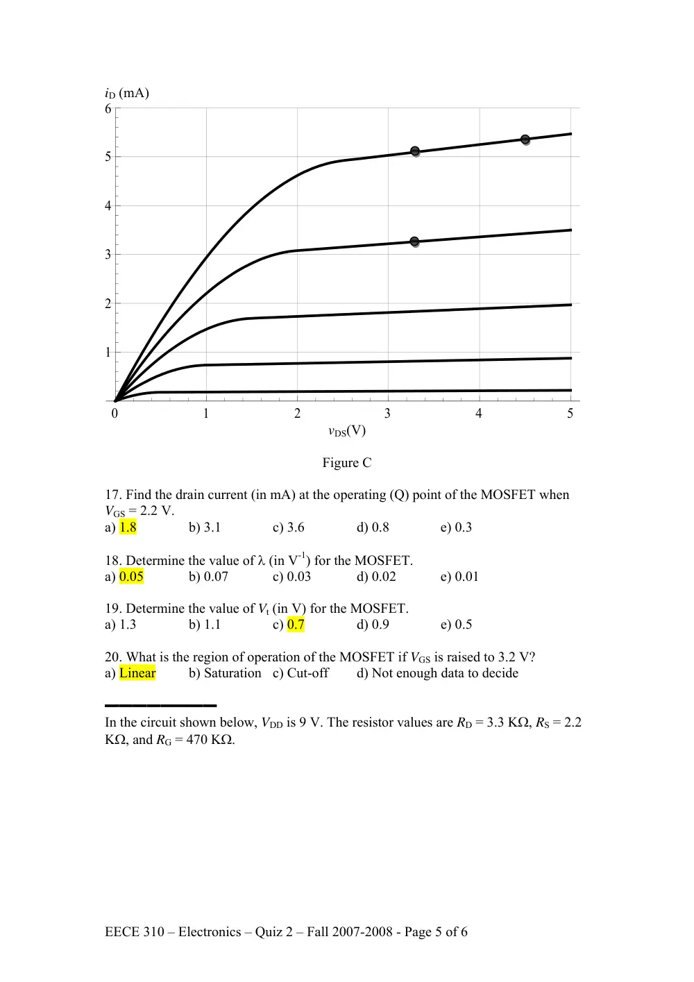
To analyze the circuit shown below, we use the MOSFET characteristics shown in
Figure C. The iD – vDS curves correspond to the following values of VGS: 1.2, 1.7, 2.2,
2.7, and 3.2 V.
The three points shown on the plot have the following coordinates (3.3 V , 3.26 mA),
(3.3 V , 5.10 mA), and (4.5 V , 5.36 mA)
Assume that VDD is 5 V and RD = 1 KΩ.
EECE 310 – Electronics – Quiz 2 – Fall 2007-2008 - Page 5 of 6
iD (mA)
0
1
2
3
4
5
1
2
3
4
5
6
vDS(V)
Figure C
17. Find the drain current (in mA) at the operating (Q) point of the MOSFET when
VGS = 2.2 V.
a) 1.8
b) 3.1
c) 3.6
d) 0.8
e) 0.3
18. Determine the value of λ (in V-1) for the MOSFET.
a) 0.05
b) 0.07
c) 0.03
d) 0.02
e) 0.01
19. Determine the value of Vt (in V) for the MOSFET.
a) 1.3
b) 1.1
c) 0.7
d) 0.9
e) 0.5
20. What is the region of operation of the MOSFET if VGS is raised to 3.2 V?
a) Linear
b) Saturation c) Cut-off
d) Not enough data to decide
▬▬▬▬▬▬▬▬
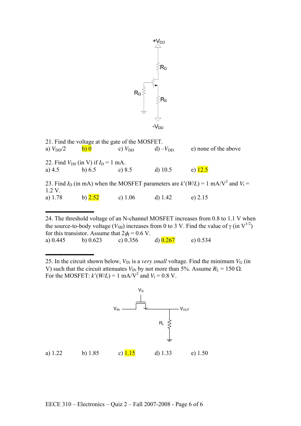
In the circuit shown below, VDD is 9 V. The resistor values are RD = 3.3 KΩ, RS = 2.2
KΩ, and RG = 470 KΩ.
EECE 310 – Electronics – Quiz 2 – Fall 2007-2008 - Page 6 of 6
21. Find the voltage at the gate of the MOSFET.
a) VDD/2
b) 0
c) VDD
d) –VDD
e) none of the above
22. Find VDS (in V) if ID = 1 mA.
a) 4.5
b) 6.5
c) 8.5
d) 10.5
e) 12.5
23. Find ID (in mA) when the MOSFET parameters are k’(W/L) = 1 mA/V2 and Vt =
1.2 V.
a) 1.78
b) 2.52
c) 1.06
d) 1.42
e) 2.15
▬▬▬▬▬▬▬▬
24. The threshold voltage of an N-channel MOSFET increases from 0.8 to 1.1 V when
the source-to-body voltage (VSB) increases from 0 to 3 V. Find the value of γ (in V1/2)
for this transistor. Assume that 2φf = 0.6 V.
a) 0.445
b) 0.623
c) 0.356
d) 0.267
e) 0.534
▬▬▬▬▬▬▬▬
25. In the circuit shown below, VIN is a very small voltage. Find the minimum VG (in
V) such that the circuit attenuates VIN by not more than 5%. Assume RL = 150 Ω.
For the MOSFET: k’(W/L) = 1 mA/V2 and Vt = 0.8 V.
VG
VIN
VOUT
RL
a) 1.22
b) 1.85
c) 1.15
d) 1.33
e) 1.50