
EECE 310 Exam 2, Fall 2007
American University of Beirut · Electronics · 6 pages


More EECE 310 files
- Midterm · Fall 2014ExamView
- Midterm with Solutions · Fall 2014Exam · with solutionView
- Midterm · Fall 2013ExamView
- Midterm · Fall 2012ExamView
- Midterm with Solution · Summer 2011Exam · with solutionView
- Exam 2 with Answers · Fall 2011Exam · with solutionView
- Exam 1 with Answers · Fall 2011Exam · with solutionView
- Exam 1 · Fall 2010ExamView
Show the text of this exam
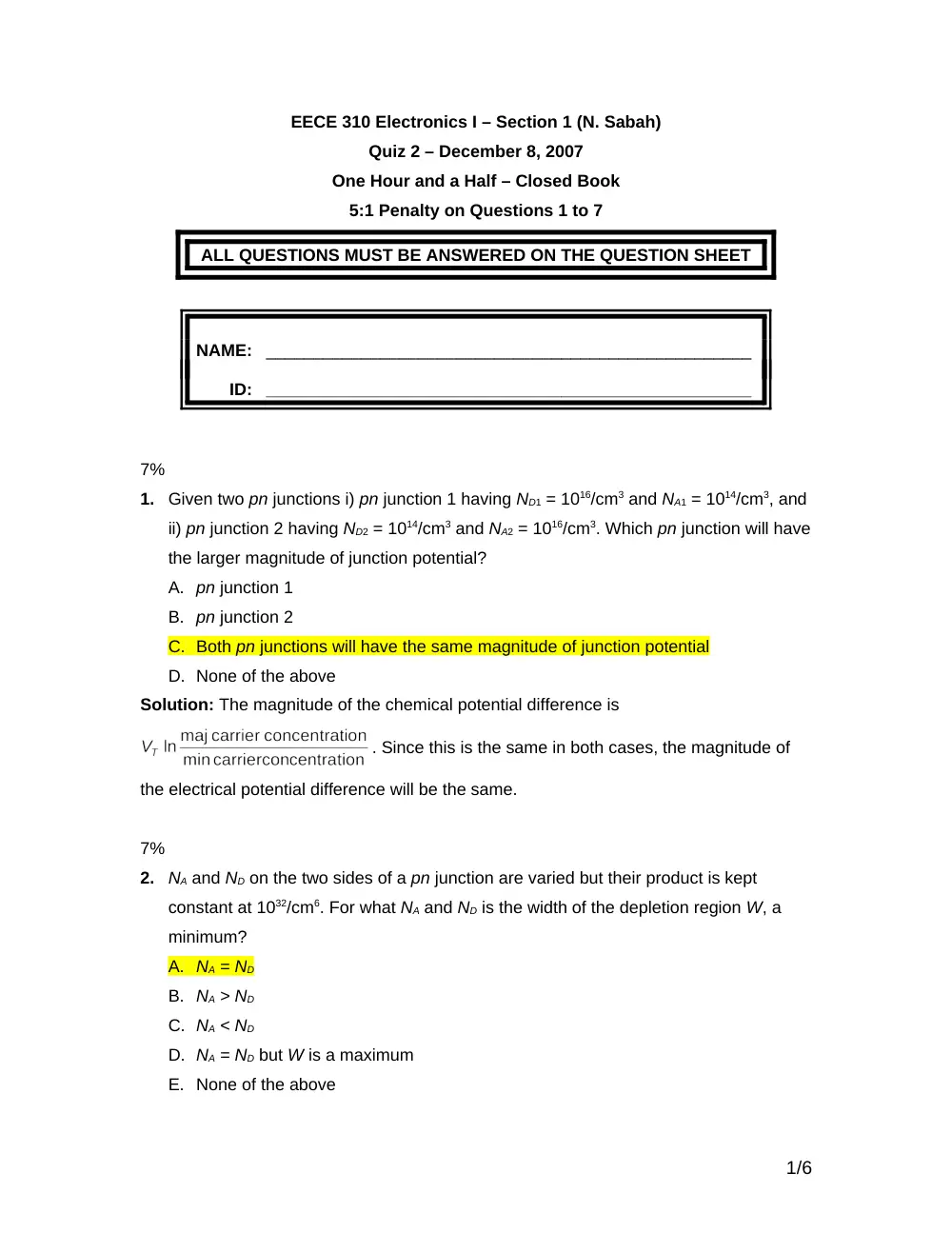
EECE 310 Electronics I – Section 1 (N. Sabah)
Quiz 2 – December 8, 2007
One Hour and a Half – Closed Book
5:1 Penalty on Questions 1 to 7
ALL QUESTIONS MUST BE ANSWERED ON THE QUESTION SHEET
NAME:
___________________________________________________
ID:
___________________________________________________
7%
1.
Given two pn junctions i) pn junction 1 having ND1 = 1016/cm3 and NA1 = 1014/cm3, and
ii) pn junction 2 having ND2 = 1014/cm3 and NA2 = 1016/cm3. Which pn junction will have
the larger magnitude of junction potential?
A. pn junction 1
B. pn junction 2
C. Both pn junctions will have the same magnitude of junction potential
D. None of the above
Solution: The magnitude of the chemical potential difference is
. Since this is the same in both cases, the magnitude of
the electrical potential difference will be the same.
7%
2.
NA and ND on the two sides of a pn junction are varied but their product is kept
constant at 1032/cm6. For what NA and ND is the width of the depletion region W, a
minimum?
A. NA = ND
B. NA > ND
C. NA < ND
D. NA = ND but W is a maximum
E. None of the above
1/6
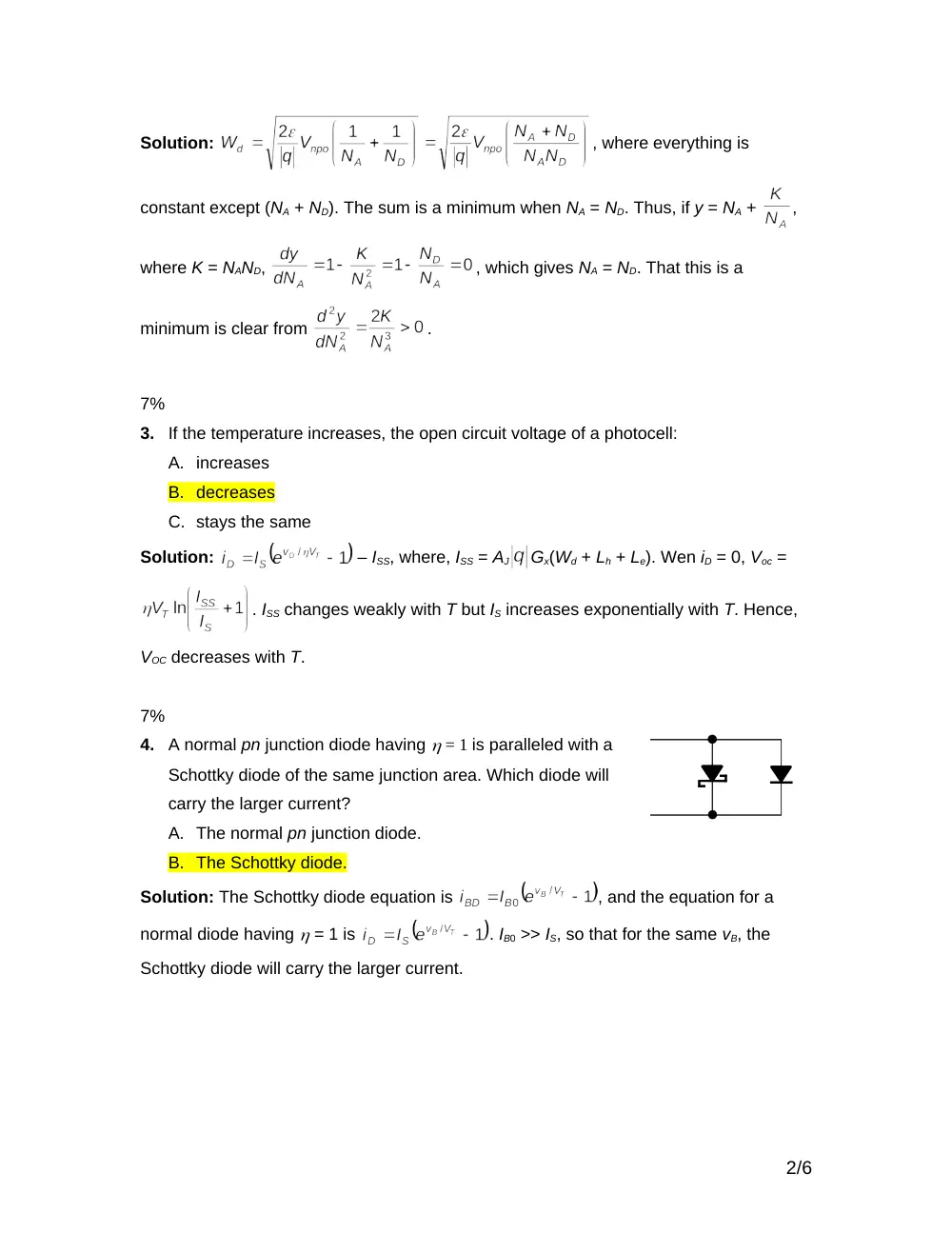
Solution:
, where everything is
constant except (NA + ND). The sum is a minimum when NA = ND. Thus, if y = NA +
,
where K = NAND,
, which gives NA = ND. That this is a
minimum is clear from
.
7%
3.
If the temperature increases, the open circuit voltage of a photocell:
A. increases
B. decreases
C. stays the same
Solution:
– ISS, where, ISS = AJ
Gx(Wd + Lh + Le). Wen iD = 0, Voc =
. ISS changes weakly with T but IS increases exponentially with T. Hence,
VOC decreases with T.
7%
4.
A normal pn junction diode having = 1 is paralleled with a
Schottky diode of the same junction area. Which diode will
carry the larger current?
A. The normal pn junction diode.
B. The Schottky diode.
Solution: The Schottky diode equation is
, and the equation for a
normal diode having = 1 is
. IB0 >> IS, so that for the same vB, the
Schottky diode will carry the larger current.
2/6
7%
5.
In the circuit shown, VDD = 5 V, Vt = 1 V, C is initially
discharged, and vI suddenly increases from zero to a steady
value VDD. The final value of vC is:
A. 5 V
B. 4 V
C. 3 V
D. 1 V
E. None of the above
Solution: When vI increases from zero to VDD, with vC = 0 initially, vGS = VDD, iD flows, C
charges, vC increases, and vGS and iD decrease. iD becomes zero when vGS = Vt. The final
value of vC is therefore, VDD – Vt = 5 – 1 = 4V.
7%
6.
The E-NMOS transistor has
A / V2,
, Vtn =
1 V and = 0. If it is replaced by a D-NMOS transistor whose
transfer characteristic is that of the E-NMOS transistor shifted
by 3 V, the D-NMOS transistor will be:
A. in the triode region
B. in the saturation region
C. cut-off
D. None of the above
Solution: VGS = 2 V, VtnD = 1 – 3 = -2 V; assuming transistor is in
saturation,
mA. This makes vDS < 0, which means the
assumption is wrong and the transistor is in the triode region. To confirm this, iD and vDS
can be found by solving the equations:
and vDS + iD = 5.
This gives
mA, vDS = 1.13 V; vDS < vGS – VtnD, which confirms that
transistor is in triode region.
3/6
1 k
+5 V
3 k
2 k
VDD
vI
vC
+
–
+
–
C
7%
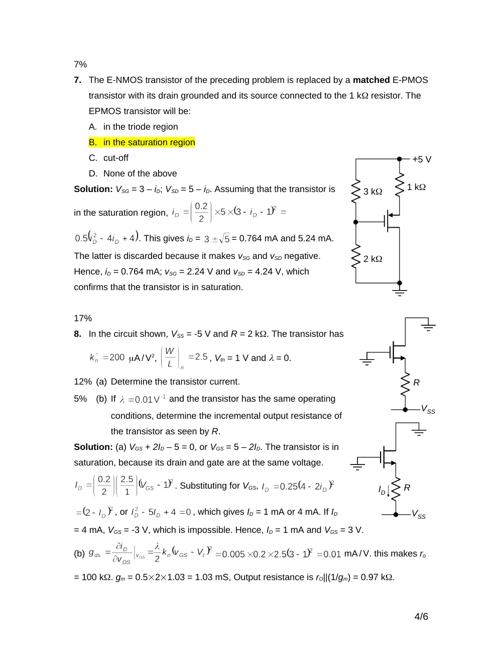
7.
The E-NMOS transistor of the preceding problem is replaced by a matched E-PMOS
transistor with its drain grounded and its source connected to the 1 k resistor. The
EPMOS transistor will be:
A. in the triode region
B. in the saturation region
C. cut-off
D. None of the above
Solution: VSG = 3 – iD; VSD = 5 – iD. Assuming that the transistor is
in the saturation region,
. This gives iD =
= 0.764 mA and 5.24 mA.
The latter is discarded because it makes vSG and vSD negative.
Hence, iD = 0.764 mA; vSG = 2.24 V and vSD = 4.24 V, which
confirms that the transistor is in saturation.
17%
8.
In the circuit shown, VSS = -5 V and R = 2 k. The transistor has
A / V2,
, Vtn = 1 V and = 0.
12% (a) Determine the transistor current.
5%
(b) If
and the transistor has the same operating
conditions, determine the incremental output resistance of
the transistor as seen by R.
Solution: (a) VGS + 2ID – 5 = 0, or VGS = 5 – 2ID. The transistor is in
saturation, because its drain and gate are at the same voltage.
. Substituting for VGS,
, or
, which gives ID = 1 mA or 4 mA. If ID
= 4 mA, VGS = -3 V, which is impossible. Hence, ID = 1 mA and VGS = 3 V.
(b)
mA / V. this makes ro
= 100 k. gm = 0.521.03 = 1.03 mS, Output resistance is rO||(1/gm) = 0.97 k.
4/6
R
VSS
R
VSS
ID
1 k
+5 V
3 k
2 k
17%
9.
In the circuit shown, Q1 and Q2 have
mA / V2, Vt
= 0.8 V,
,
0.05 V-1, (W/L)n1 = 10, and (W/L)n2
= 20. Determine IO.
Solution: Q1 is in saturation, so 1 =
;
hence,
V. Assuming Q2 is in
saturation, IO =
= 2 + 0.1VDS2. From
KVL, VDS2 + 0.5IO = 5, or VDS2 = 5 – 0.5IO. Substituting, IO = 2.38 mA and VDS2 = 3.81 V,
which confirms that Q2 is in saturation.
17%
10. The transistors of a CMOS inverter operating from a VDD = 3 V supply have the
following parameters:
E-NMOS:
120 A/V2,
(W/L)n = 4
Vtn = 0.6 V
= 0
E-PMOS:
50 A/V2,
(W/L)p = 6
Vtp = -0.7 V
= 0
Determine the input voltage vI that makes the inverter operate on the vertical
segment of its transfer characteristic.
Solution: Over the vertical segment of the transfer characteristic, both transistors
operate in the saturation region, with equal currents. For Qn: iDn =
. For Qp:
. Equating
the currents:
, or
. This
gives
V, or -5.81 V. The negative value is discarded, so that
vI = 1.35 V.
5/6
500
+5V
Q1
Q2
1 mA
IO
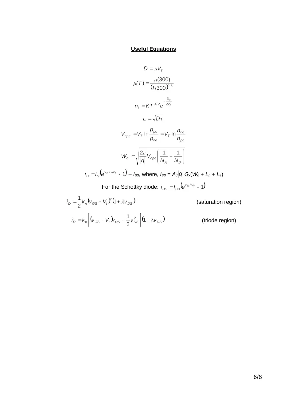
Useful Equations
– ISS, where, ISS = AJ
Gx(Wd + Lh + Le)
For the Schottky diode:
(saturation region)
(triode region)
6/6