
EECE 310 Exam 2, Fall 2008
American University of Beirut · Electronics · 7 pages


More EECE 310 files
- Midterm · Fall 2014ExamView
- Midterm with Solutions · Fall 2014Exam · with solutionView
- Midterm · Fall 2013ExamView
- Midterm · Fall 2012ExamView
- Exam 2 with Answers · Fall 2011Exam · with solutionView
- Midterm with Solution · Summer 2011Exam · with solutionView
- Exam 1 with Answers · Fall 2011Exam · with solutionView
- Exam 1 · Fall 2010ExamView
Show the text of this exam
EECE 310 – Electronics – Quiz 2 – Fall 2008-2009 - Page 1 of 7
American University of Beirut
Department of Electrical and Computer Engineering
EECE 310 – Electronics
Quiz 2 – December 19, 2008
Closed Book – No Programmable Calculators
90 minutes
Penalty is 5 to 1
(1 to 4 wrong answers do not result in a penalty; 5 to 9 wrong answers cancel one
correct answer; 10 to 14 wrong answers cancel two correct answers; and so on)
Name: _________ANSWERS________________ ID number: _________________
EECE 310 – Electronics – Quiz 2 – Fall 2008-2009 - Page 2 of 7
An N-channel MOSFET with k’ = 1 mA/V2 is biased such that it is operating in the
saturation region. The Early voltage for this MOSFET is VA = 5 V.
When the MOSFET is biased at VOV = 1 V, with VDS = VX Volts, the drain current is
1 mA. When the overdrive voltage increases to 1.2 V, VDS decreases by 20% to
0.8×VX while the drain current increases to 1.2 mA.
1. Find the initial value of VDS (VX in V).
a) 35
b) 32.5
c) 27.5
d) 25
e) 30
2. Find the value of (W/L) for this MOSFET.
a) 1/6
b) 1/7
c) 1/4
d) 1/3
e) 1/5
▬▬▬▬▬▬▬▬
3. If a P-channel MOSFET is biased at VGS = –9 V and VDS = –1 V, and has a
threshold voltage Vt = –3 V, find its region of operation.
a) Triode (Linear) b) Saturation c) Cutoff d) Pinch-Off e) Unknown
▬▬▬▬▬▬▬▬
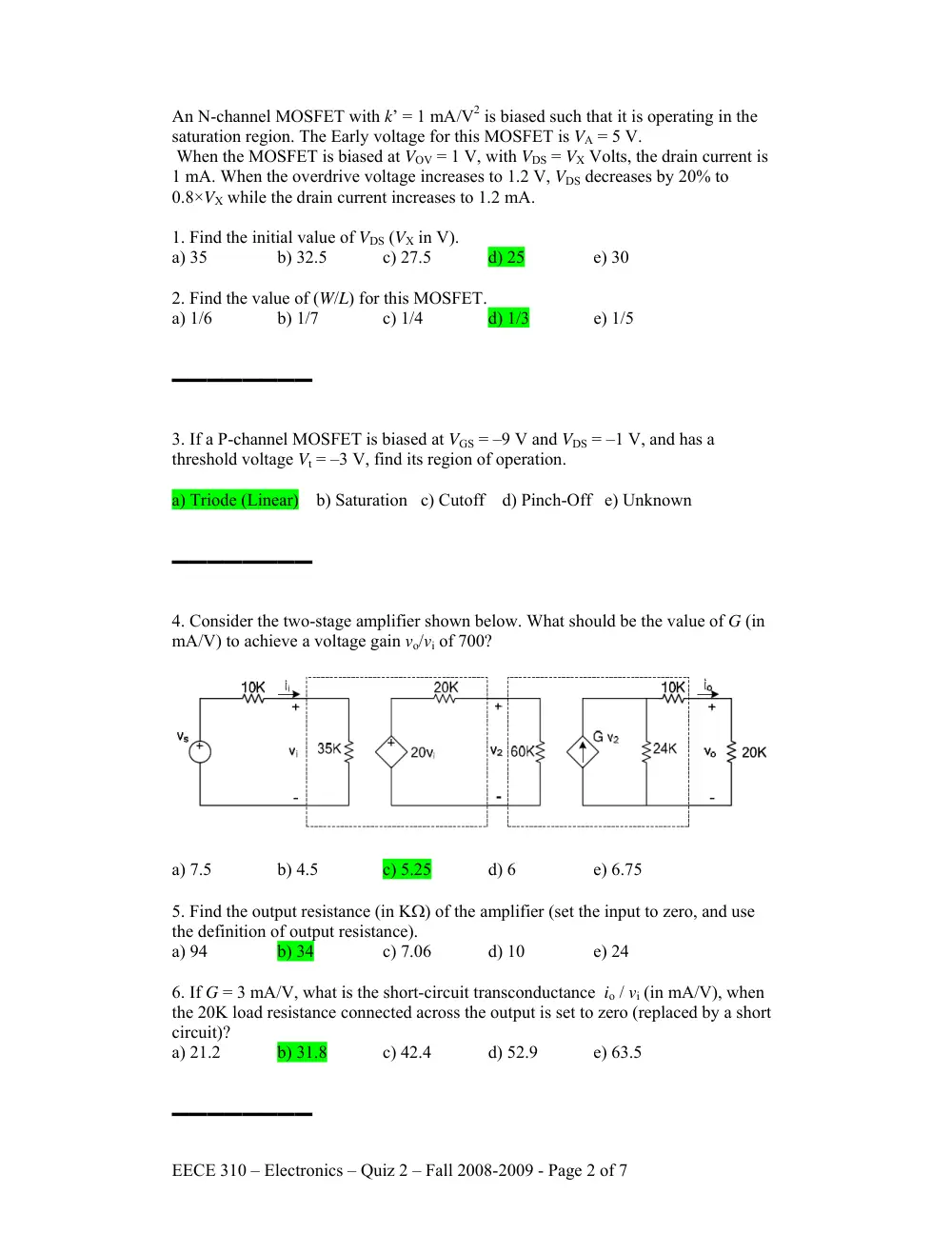
4. Consider the two-stage amplifier shown below. What should be the value of G (in
mA/V) to achieve a voltage gain vo/vi of 700?
a) 7.5
b) 4.5
c) 5.25
d) 6
e) 6.75
5. Find the output resistance (in KΩ) of the amplifier (set the input to zero, and use
the definition of output resistance).
a) 94
b) 34
c) 7.06
d) 10
e) 24
6. If G = 3 mA/V, what is the short-circuit transconductance io / vi (in mA/V), when
the 20K load resistance connected across the output is set to zero (replaced by a short
circuit)?
a) 21.2
b) 31.8
c) 42.4
d) 52.9
e) 63.5
▬▬▬▬▬▬▬▬
EECE 310 – Electronics – Quiz 2 – Fall 2008-2009 - Page 3 of 7
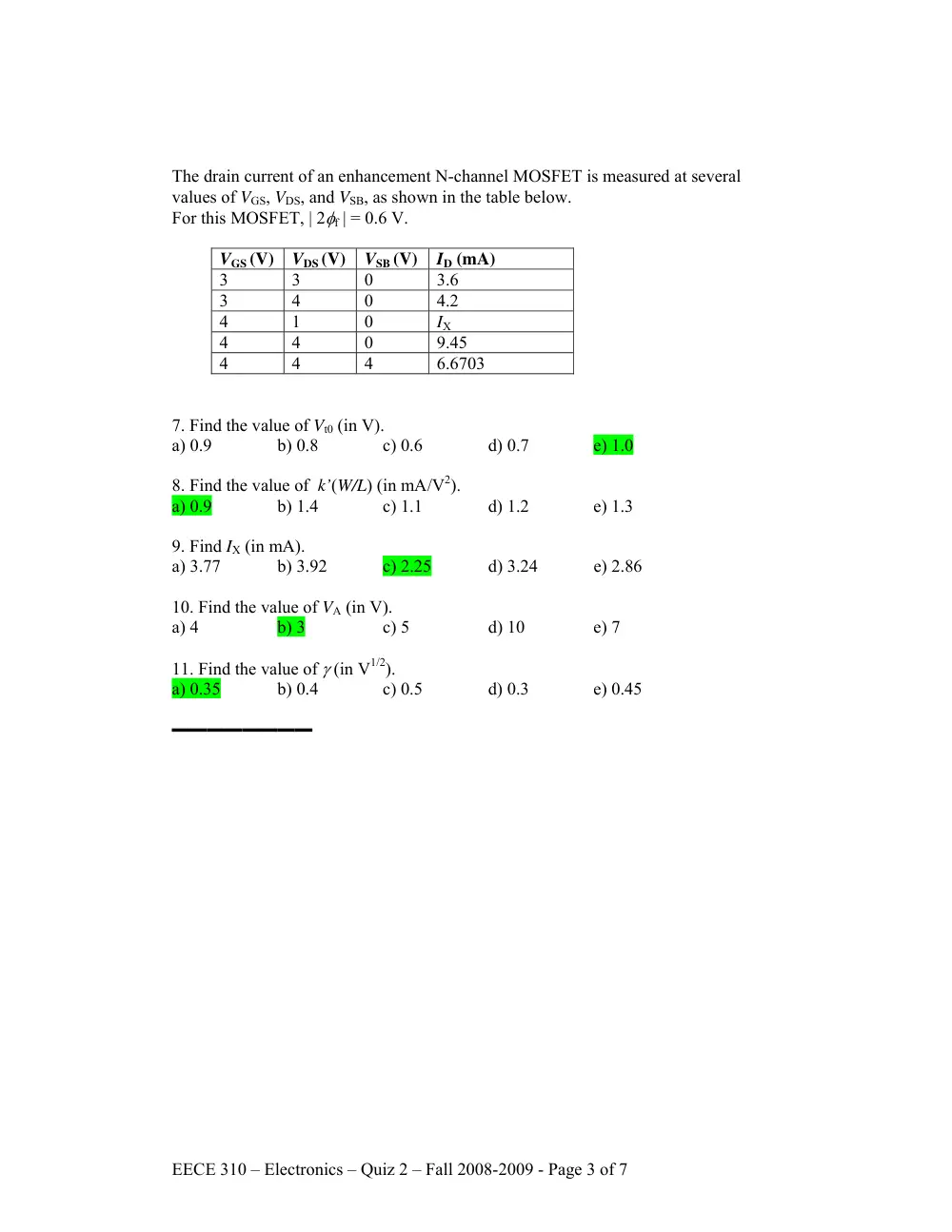
The drain current of an enhancement N-channel MOSFET is measured at several
values of VGS, VDS, and VSB, as shown in the table below.
For this MOSFET, | 2φf | = 0.6 V.
VGS (V) VDS (V)
VSB (V)
ID (mA)
3
3
0
3.6
3
4
0
4.2
4
1
0
IX
4
4
0
9.45
4
4
4
6.6703
7. Find the value of Vt0 (in V).
a) 0.9
b) 0.8
c) 0.6
d) 0.7
e) 1.0
8. Find the value of k’(W/L) (in mA/V2).
a) 0.9
b) 1.4
c) 1.1
d) 1.2
e) 1.3
9. Find IX (in mA).
a) 3.77
b) 3.92
c) 2.25
d) 3.24
e) 2.86
10. Find the value of VA (in V).
a) 4
b) 3
c) 5
d) 10
e) 7
11. Find the value of γ (in V1/2).
a) 0.35
b) 0.4
c) 0.5
d) 0.3
e) 0.45
▬▬▬▬▬▬▬▬
EECE 310 – Electronics – Quiz 2 – Fall 2008-2009 - Page 4 of 7
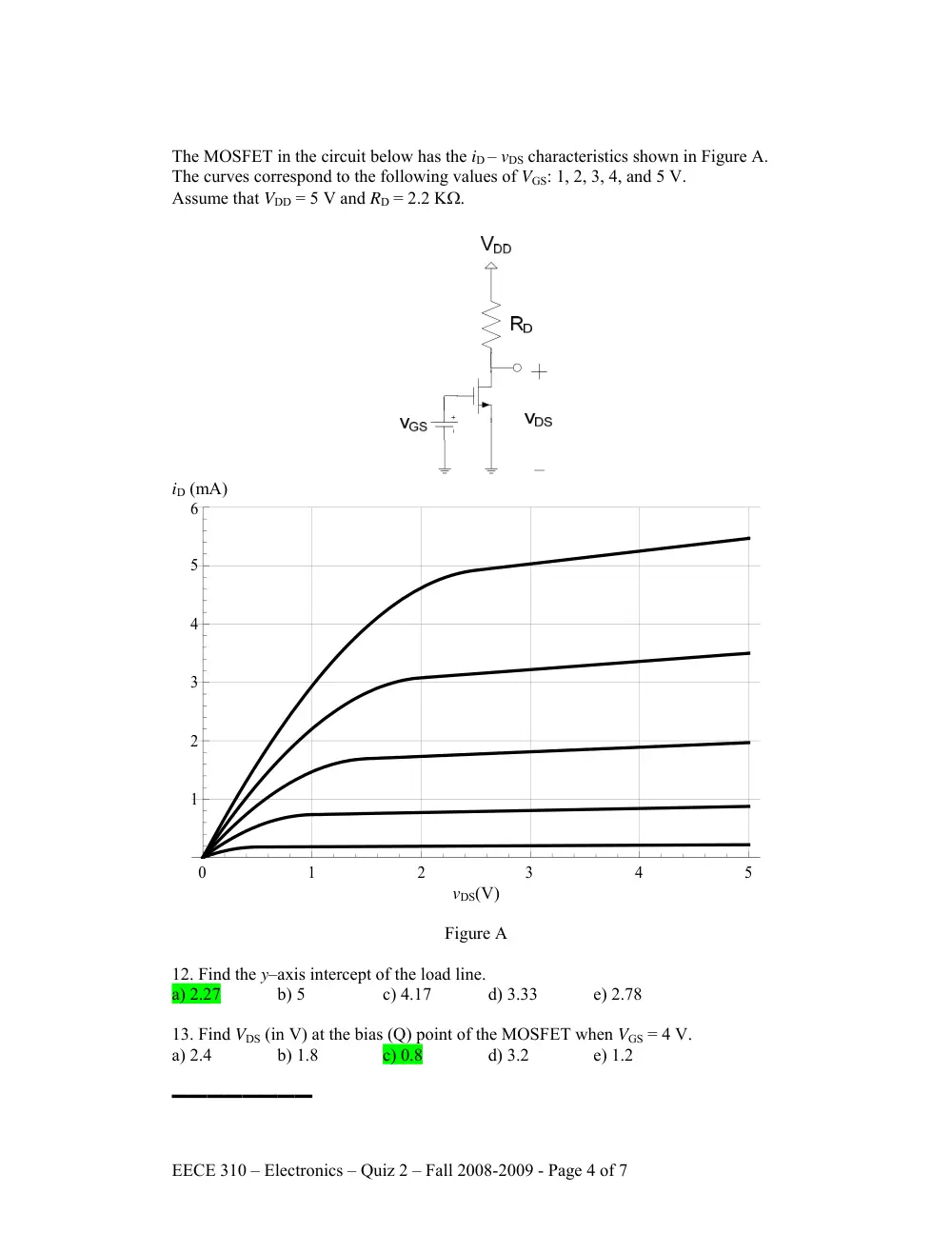
The MOSFET in the circuit below has the iD – vDS characteristics shown in Figure A.
The curves correspond to the following values of VGS: 1, 2, 3, 4, and 5 V.
Assume that VDD = 5 V and RD = 2.2 KΩ.
iD (mA)
0
1
2
3
4
5
1
2
3
4
5
6
vDS(V)
Figure A
12. Find the y–axis intercept of the load line.
a) 2.27
b) 5
c) 4.17
d) 3.33
e) 2.78
13. Find VDS (in V) at the bias (Q) point of the MOSFET when VGS = 4 V.
a) 2.4
b) 1.8
c) 0.8
d) 3.2
e) 1.2
▬▬▬▬▬▬▬▬
EECE 310 – Electronics – Quiz 2 – Fall 2008-2009 - Page 5 of 7
14. Find the drain current (in mA) for the MOSFET in the circuit below. The
MOSFET parameters are Vt0 = 1 V, k’(W/L) = 1 mA/V2, and VA = 4 V.
Assume VGS = 3 V, VDD = 9 V and RD = 1 KΩ.
a) 0.39
b) 1.44
c) 2.85
d) 4.33
e) 5.70
▬▬▬▬▬▬▬▬
15. Find VGS (in V) for the MOSFET in the circuit below. The MOSFET parameters
are Vt0 = 0.8 V and k’(W/L) = 0.2 mA/V2. Assume RS = 0.5 KΩ.
a) 3.67
b) 4.37
c) 3.99
d) 3.27
e) 3.02
9V
3.3K
1000K
RS
1000K
▬▬▬▬▬▬▬▬
EECE 310 – Electronics – Quiz 2 – Fall 2008-2009 - Page 6 of 7
16. The drain current for the MOSFET in the circuit shown is given by VDD/2R. The
MOSFET threshold voltage is –VDD/8. Find the product k’(W/L) × VDD × R.
a) 6.6
b) 11.1
c) 9.0
d) 7.84
e) 7.1
R
VDD
▬▬▬▬▬▬▬▬
17. Assume in the circuit below that vi is a small voltage, not exceeding a few
milliVolts. Find the value of (W/L) for the MOSFET, if it is required to have
vo/vi = 0.5 when VGG = 1.8 V.
The MOSFET parameters are Vt0 = 0.6 V and k’ = 0.1 mA/V2.
a) 4.76
b) 3.70
c) 11.1
d) 8.33
e) 6.25
▬▬▬▬▬▬▬▬
18. A MOSFET amplifier is biased at VOV = 0.1×VDD, VDS = 0.5×VDD. Find the
product gm×ro for this MOSFET, if VA = 4×VDD.
a) 150
b) 170
c) 90
d) 110
e) 130
▬▬▬▬▬▬▬▬
EECE 310 – Electronics – Quiz 2 – Fall 2008-2009 - Page 7 of 7
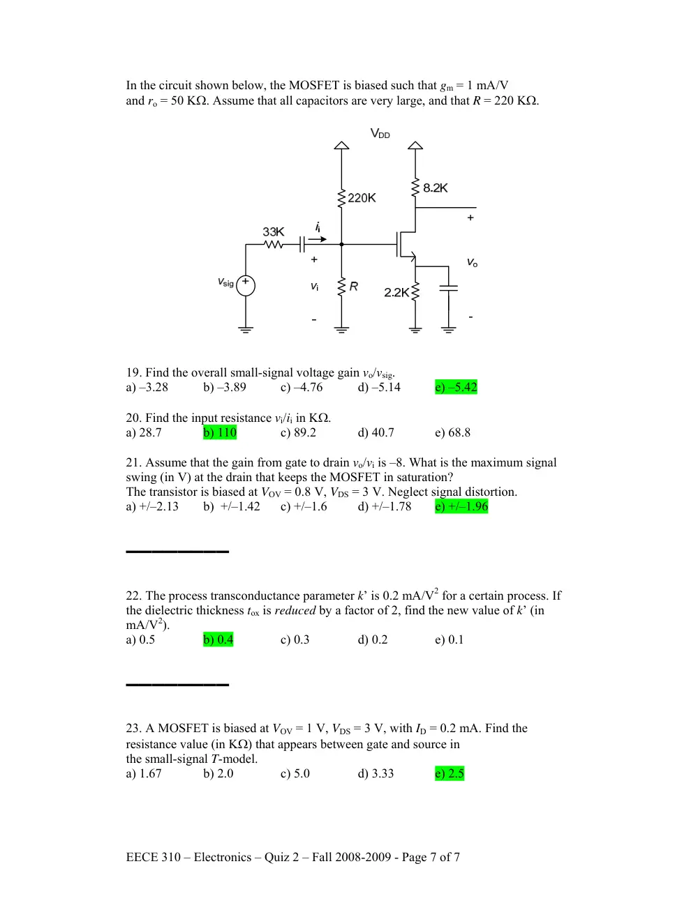
In the circuit shown below, the MOSFET is biased such that gm = 1 mA/V
and ro = 50 KΩ. Assume that all capacitors are very large, and that R = 220 KΩ.
19. Find the overall small-signal voltage gain vo/vsig.
a) –3.28
b) –3.89
c) –4.76
d) –5.14
e) –5.42
20. Find the input resistance vi/ii in KΩ.
a) 28.7
b) 110
c) 89.2
d) 40.7
e) 68.8
21. Assume that the gain from gate to drain vo/vi is –8. What is the maximum signal
swing (in V) at the drain that keeps the MOSFET in saturation?
The transistor is biased at VOV = 0.8 V, VDS = 3 V. Neglect signal distortion.
a) +/–2.13
b) +/–1.42
c) +/–1.6
d) +/–1.78
e) +/–1.96
▬▬▬▬▬▬▬▬
22. The process transconductance parameter k’ is 0.2 mA/V2 for a certain process. If
the dielectric thickness tox is reduced by a factor of 2, find the new value of k’ (in
mA/V2).
a) 0.5
b) 0.4
c) 0.3
d) 0.2
e) 0.1
▬▬▬▬▬▬▬▬
23. A MOSFET is biased at VOV = 1 V, VDS = 3 V, with ID = 0.2 mA. Find the
resistance value (in KΩ) that appears between gate and source in
the small-signal T-model.
a) 1.67
b) 2.0
c) 5.0
d) 3.33
e) 2.5