
EECE 310 Exam 2, Fall 2009
American University of Beirut · Electronics · 7 pages

More EECE 310 files
- Midterm · Fall 2014ExamView
- Midterm with Solutions · Fall 2014Exam · with solutionView
- Midterm · Fall 2013ExamView
- Midterm · Fall 2012ExamView
- Exam 2 with Answers · Fall 2011Exam · with solutionView
- Midterm with Solution · Summer 2011Exam · with solutionView
- Exam 1 with Answers · Fall 2011Exam · with solutionView
- Exam 1 · Fall 2010ExamView
Show the text of this exam
EECE 310 – Electronics – Quiz 2 – Fall 2009-2010 - Page 1 of 7
American University of Beirut
Department of Electrical and Computer Engineering
EECE 310 – Electronics
Quiz 2 – December 19, 2009
Closed Book – No Programmable Calculators
90 minutes
Penalty is 5 to 1
(1 to 4 wrong answers do not result in a penalty; 5 to 9 wrong answers cancel one
correct answer; 10 to 14 wrong answers cancel two correct answers; and so on)
Name: _________________________________
ID number: _________________
EECE 310 – Electronics – Quiz 2 – Fall 2009-2010 - Page 2 of 7
Two voltage amplifiers are cascaded to amplify the voltage signal of a source vi and
deliver it to a load RL = 50 kΩ.
The first amplifier is modeled by an input resistance Ri = 160 kΩ, output resistance
Ro = 10 kΩ, and open-circuit voltage gain Avo = 100 V/V.
The second amplifier is modeled by Ri = 20 kΩ, output resistance Ro = 40 kΩ,
and Avo = 30 V/V.
1. Find the voltage gain vo/vi (in V/V), where vo is the voltage across RL.
a) 1000
b) 1667
c) 1429
d) 1250
e) 1111
2. Considering the two cascaded amplifiers as one equivalent amplifier, what is the
input resistance (in kΩ) of this equivalent amplifier?
a) 100
b) 120
c) 140
d) 160
e) 180
3. Considering the two cascaded amplifiers as one equivalent amplifier, what is the
output resistance (in kΩ) of this equivalent amplifier?
a) 40
b) 50
c) 10
d) 20
e) 30
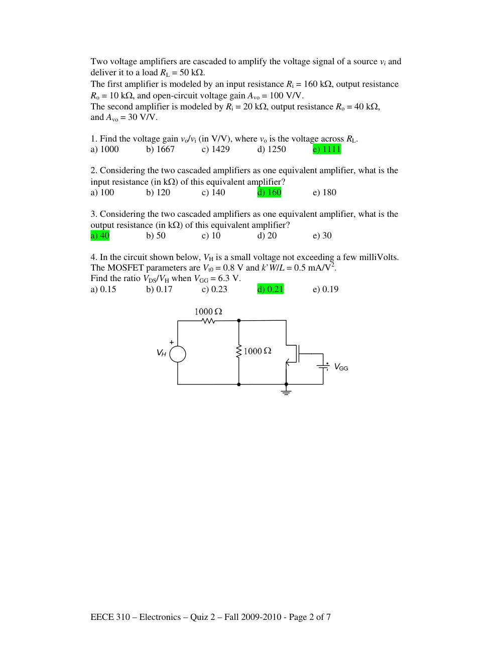
4. In the circuit shown below, VH is a small voltage not exceeding a few milliVolts.
The MOSFET parameters are Vt0 = 0.8 V and k’W/L = 0.5 mA/V2.
Find the ratio VDS/VH when VGG = 6.3 V.
a) 0.15
b) 0.17
c) 0.23
d) 0.21
e) 0.19
EECE 310 – Electronics – Quiz 2 – Fall 2009-2010 - Page 3 of 7
iD (mA)
0
1
2
3
4
5
2
4
6
8
10
vDS(V)
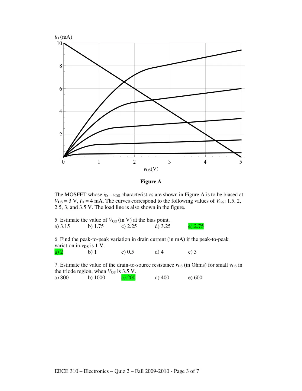
Figure A
The MOSFET whose iD – vDS characteristics are shown in Figure A is to be biased at
VDS = 3 V, ID = 4 mA. The curves correspond to the following values of VGS: 1.5, 2,
2.5, 3, and 3.5 V. The load line is also shown in the figure.
5. Estimate the value of VGS (in V) at the bias point.
a) 3.15
b) 1.75
c) 2.25
d) 3.25
e) 2.75
6. Find the peak-to-peak variation in drain current (in mA) if the peak-to-peak
variation in vDS is 1 V.
a) 2
b) 1
c) 0.5
d) 4
e) 3
7. Estimate the value of the drain-to-source resistance rDS (in Ohms) for small vDS in
the triode region, when VGS is 3.5 V.
a) 800
b) 1000
c) 200
d) 400
e) 600
EECE 310 – Electronics – Quiz 2 – Fall 2009-2010 - Page 4 of 7
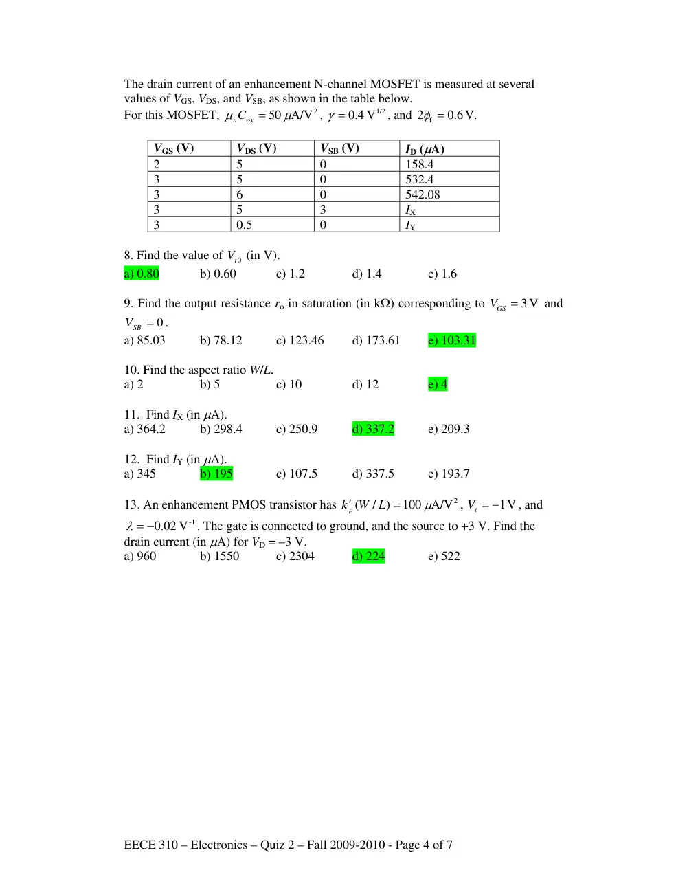
The drain current of an enhancement N-channel MOSFET is measured at several
values of VGS, VDS, and VSB, as shown in the table below.
For this MOSFET,
A/V2
50 μ
μ
nCox =
,
V1/2
4.0
γ =
, and
6.0
2 f =
φ
V.
VGS (V)
VDS (V)
VSB (V)
ID (μA)
2
5
0
158.4
3
5
0
532.4
3
6
0
542.08
3
5
3
IX
3
0.5
0
IY
8. Find the value of
0
tV (in V).
a) 0.80
b) 0.60
c) 1.2
d) 1.4
e) 1.6
9. Find the output resistance ro in saturation (in kΩ) corresponding to
3 V
VGS =
and
VSB = 0
.
a) 85.03
b) 78.12
c) 123.46
d) 173.61
e) 103.31
10. Find the aspect ratio W/L.
a) 2
b) 5
c) 10
d) 12
e) 4
11. Find IX (in μA).
a) 364.2
b) 298.4
c) 250.9
d) 337.2
e) 209.3
12. Find IY (in μA).
a) 345
b) 195
c) 107.5
d) 337.5
e) 193.7
13. An enhancement PMOS transistor has
100 A/V2
/ )
(
μ
=
′
k p W L
,
tV = − 1V
, and
λ = − .0 02 V-1
. The gate is connected to ground, and the source to +3 V. Find the
drain current (in μA) for VD = –3 V.
a) 960
b) 1550
c) 2304
d) 224
e) 522
EECE 310 – Electronics – Quiz 2 – Fall 2009-2010 - Page 5 of 7
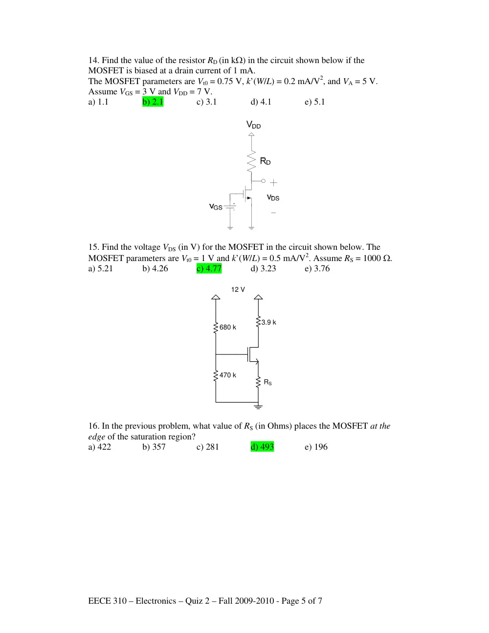
14. Find the value of the resistor RD (in kΩ) in the circuit shown below if the
MOSFET is biased at a drain current of 1 mA.
The MOSFET parameters are Vt0 = 0.75 V, k’(W/L) = 0.2 mA/V2, and VA = 5 V.
Assume VGS = 3 V and VDD = 7 V.
a) 1.1
b) 2.1
c) 3.1
d) 4.1
e) 5.1
15. Find the voltage VDS (in V) for the MOSFET in the circuit shown below. The
MOSFET parameters are Vt0 = 1 V and k’(W/L) = 0.5 mA/V2. Assume RS = 1000 Ω.
a) 5.21
b) 4.26
c) 4.77
d) 3.23
e) 3.76
12 V
3.9 k
680 k
RS
470 k
16. In the previous problem, what value of RS (in Ohms) places the MOSFET at the
edge of the saturation region?
a) 422
b) 357
c) 281
d) 493
e) 196
EECE 310 – Electronics – Quiz 2 – Fall 2009-2010 - Page 6 of 7
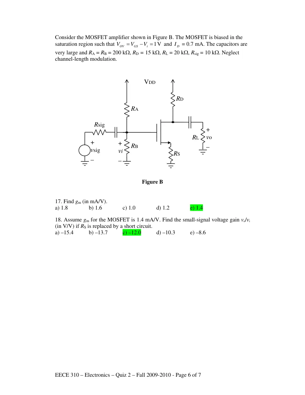
Consider the MOSFET amplifier shown in Figure B. The MOSFET is biased in the
saturation region such that
= 1V
−
=
t
GS
OV
V
V
V
and
D
I = 0.7 mA. The capacitors are
very large and RA = RB = 200 kΩ, RD = 15 kΩ, RL = 20 kΩ, Rsig = 10 kΩ. Neglect
channel-length modulation.
Figure B
17. Find gm (in mA/V).
a) 1.8
b) 1.6
c) 1.0
d) 1.2
e) 1.4
18. Assume gm for the MOSFET is 1.4 mA/V. Find the small-signal voltage gain vo/vi
(in V/V) if RS is replaced by a short circuit.
a) –15.4
b) –13.7
c) –12.0
d) –10.3
e) –8.6
+
vsig
_
Rsig
RA
RB
RD
RL
+
vo
_
VDD
+
vi
_
RS
EECE 310 – Electronics – Quiz 2 – Fall 2009-2010 - Page 7 of 7
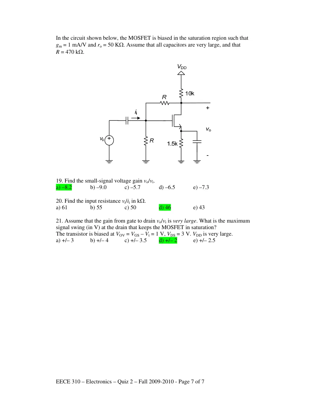
In the circuit shown below, the MOSFET is biased in the saturation region such that
gm = 1 mA/V and ro = 50 KΩ. Assume that all capacitors are very large, and that
R = 470 kΩ.
19. Find the small-signal voltage gain vo/vi.
a) –8.2
b) –9.0
c) –5.7
d) –6.5
e) –7.3
20. Find the input resistance vi/ii in kΩ.
a) 61
b) 55
c) 50
d) 46
e) 43
21. Assume that the gain from gate to drain vo/vi is very large. What is the maximum
signal swing (in V) at the drain that keeps the MOSFET in saturation?
The transistor is biased at VOV = VGS – Vt = 1 V, VDS = 3 V. VDD is very large.
a) +/– 3
b) +/– 4
c) +/– 3.5
d) +/– 2
e) +/– 2.5