
EECE 310 Exam, Spring 2008
American University of Beirut · Electronics · 9 pages



More EECE 310 files
- Midterm · Fall 2014ExamView
- Midterm with Solutions · Fall 2014Exam · with solutionView
- Midterm · Fall 2013ExamView
- Midterm · Fall 2012ExamView
- Midterm with Solution · Summer 2011Exam · with solutionView
- Exam 2 with Answers · Fall 2011Exam · with solutionView
- Exam 1 with Answers · Fall 2011Exam · with solutionView
- Exam 1 · Fall 2010ExamView
Show the text of this exam
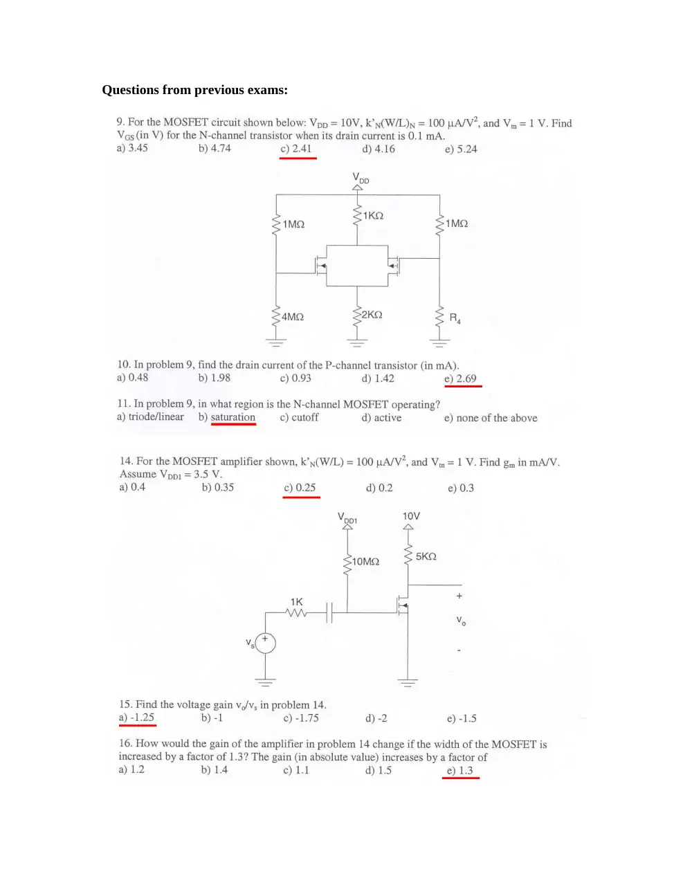
Questions from previous exams:
9. For the MOSFET circuit shown below: Vpp = 10V, k’n(W/L)x = 100
Vgs (in V) for the N-channel transistor when its drain current is 0.1 mA.
a) 3.45 b) 4.74 c)2.41 d) 4.16
Voo
a
1 KQ
= 1Ma
ral
Is +
4
Sama 2KQ
uA/V?, and V,, = 1 V. Find
e) 5.24
= 1Mo
10. In problem 9, find the drain current of the P-channel transistor (in mA).
d) 1.42
b) 1.98 c) 0.93
a) 0.48
11. In problem 9, in what region is the N-channel MOSFET operating?
a) triode/linear _b) saturation c) cutoff d) active
e) 2.69
e) none of the above
14. For the MOSFET amplifier shown, k’y(W/L) = 100 vA/Y?, and V,, = 1 V. Find g,, in mA/V.
Assume Vpp; = 3.5 V.
a) 0.4 b) 0.35 c) 0.25 d) 0.2
Mies, 10V
10M mG
mit :
WN If 4
)
15. Find the voltage gain v,/v, in problem 14.
a) -1.25 b) -1 c) -1.75 d) -2
e) 0.3
e)-1.5
16. How would the gain of the amplifier in problem 14 change if the width of the MOSFET is
increased by a factor of 1.3? The gain (in absolute value) increases by a factor of
c) Ll d) 1.5
a) 1.2 b) 1.4
e) 13
30. A CMOS inverter powered by a Vpp = 2.5 V supply uses an N-channel MOSFET with k’y(W/L)n
=2 mA/V’, Via = 0.7 V, and a P-channel MOSFET with k’p(W/L)p = 1 mA/V?, Vip = —0.8 V. Find the
output LOW voltage level (in V)
a) 0.076 b) 0.131 c)0 d) 0.101 e) 0.128
31. The inverter in problem 30 is loaded by a load that sources 1 mA from Vpp into the output. What is
the output voltage (in V) in this case? The input is HIGH.
a) 0.303 b) 0.185 c) 0.155 d) 0.229 e) 0.134
32. What is the dynamic power dissipation (in mW) of the CMOS inverter in problem 30 when it is
loaded by a 1 pF capacitor and its input is a 16 MHz clock.
a) 0.324 b) 0.1 c) 0.256 d) 0.144 e) 0.196
33. The propagation delay of the CMOS inverter in problem 30 is 1 ns when loaded by a 1 pF
capacitor. What happens to the propagation delay when the load capacitance is reduced to 0.5 pF? The
delay is
a) unchanged b) increased to 2ns c) reduced to 0.5 ns
d) increased to 4 ns e) reduced to 0.25 ns
35. The three transistors are identical except that the W/L ratio of Q, is 5 times that of Q, and Q3.
Given that k’,(W/L) = 0.2 mA/V? for Q, and Qs, with V,= 1 V for all three transistors, determine I, (in
mA).
a) 2.4 b) 0.8 c) 1.6 d)2 e) 12
+15V
1kQ 1kA<S
ay Fr a,
= ei,
sell
36. Find the product gr, for a MOSFET biased at Vas — V, = 2.3 V. The channel length modulation
parameter A is 0.01 V7.
a) 86.96 b) 83.33 c) 80.00 d) 76.92 e) 90.90
37. The transistor in the circuit shown is n-channel depletion type having k’,(W/L) = 4/3 mA/V? and
V,=—3 V. Determine the transistor current (in mA).
a)6 b) 1.5 ce) 2.5 a4 e) 0.5
p—— +15 V
5kO
—C
1 MS S1ka
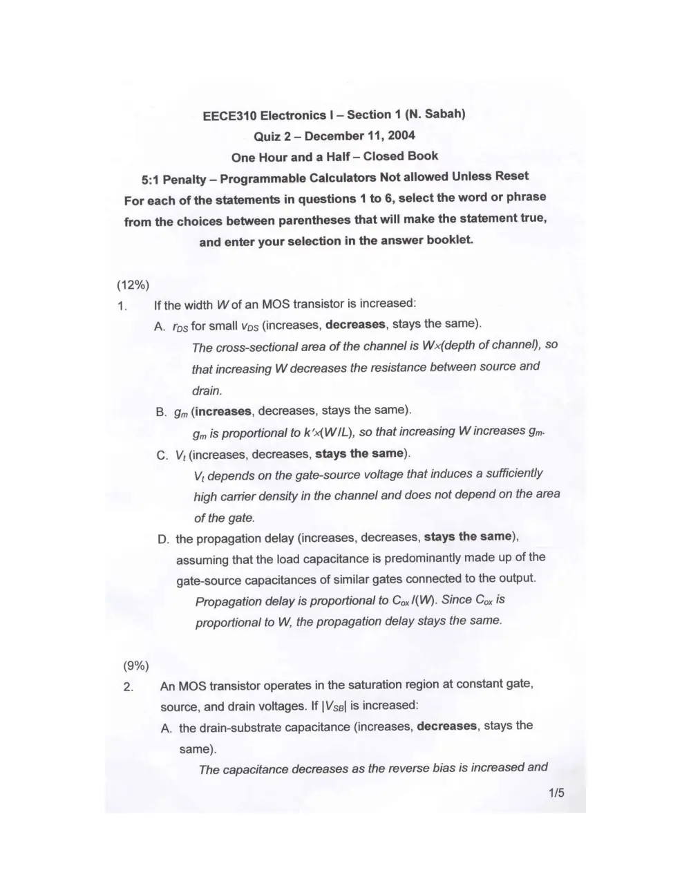
EECE310 Electronics | — Section 1 (N. Sabah)
Quiz 2 — December 11, 2004
One Hour and a Half — Closed Book
5:1 Penalty — Programmable Calculators Not allowed Unless Reset
For each of the statements in questions 1 to 6, select the word or phrase
from the choices between parentheses that will make the statement true,
and enter your selection in the answer booklet.
(12%)
1 If the width W of an MOS transistor is increased:
A. rps for small vps (increases, decreases, stays the same).
The cross-sectional area of the channel is Wx(depth of channel), so
that increasing W decreases the resistance between source and
drain.
B. Ym (increases, decreases, stays the same).
Qm is proportional to k’{WIL), so that increasing W increases gm.
C. V; (increases, decreases, stays the same).
V; depends on the gate-source voltage that induces a sufficiently
high carrier density in the channel and does not depend on the area
of the gate.
D. the propagation delay (increases, decreases, stays the same),
assuming that the load capacitance is predominantly made up of the
gate-source capacitances of similar gates connected to the output.
Propagation delay is proportional to Cox |(W). Since Cox is
proportional to W, the propagation delay stays the same.
(9%)
2. An MOS transistor operates in the saturation region at constant gate,
source, and drain voltages. If |Vsa| is increased:
A. the drain-substrate capacitance (increases, decreases, stays the
same).
The capacitance decreases as the reverse bias is increased and
1/5
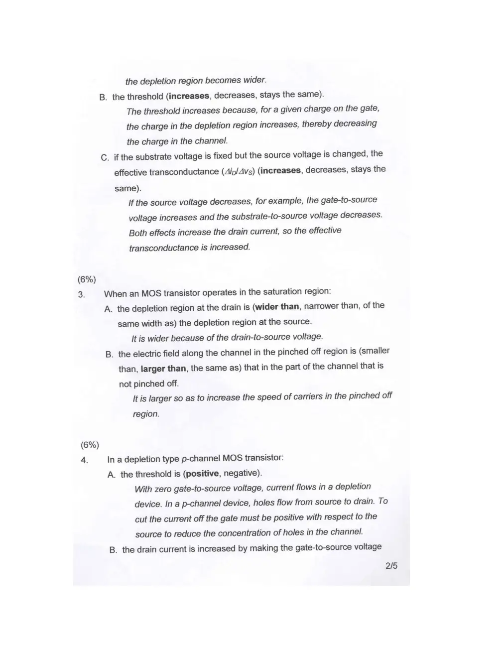
the depletion region becomes wider.
B. the threshold (increases, decreases, stays the same).
The threshold increases because, for a given charge on the gate,
the charge in the depletion region increases, thereby decreasing
the charge in the channel.
C. if the substrate voltage is fixed but the source voltage is changed, the
effective transconductance (Aip/Avs) (increases, decreases, stays the
same).
If the source voltage decreases, for example, the gate-to-source
voltage increases and the substrate-to-source voltage decreases.
Both effects increase the drain current, so the effective
transconductance is increased.
(6%)
3 When an MOS transistor operates in the saturation region:
A. the depletion region at the drain is (wider than, narrower than, of the
same width as) the depletion region at the source.
It is wider because of the drain-to-source voltage.
B. the electric field along the channel in the pinched off region is (smaller
than, larger than, the same as) that in the part of the channel that is
not pinched off.
It is larger so as to increase the speed of carriers in the pinched off
region.
(6%)
4. In a depletion type p-channel MOS transistor:
A. the threshold is (positive, negative).
With zero gate-to-source voltage, current flows in a depletion
device. In a p-channel device, holes flow from source to drain. To
cut the current off the gate must be positive with respect to the
source to reduce the concentration of holes in the channel.
B. the drain current is increased by making the gate-to-source voltage
2/5
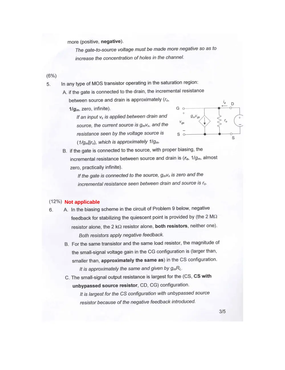
more (positive, negative).
The gate-to-source voltage must be made more negative so as to
increase the concentration of holes in the channel.
(6%)
5. In any type of MOS transistor operating in the saturation region:
A. if the gate is connected to the drain, the incremental resistance
between source and drain is approximately (ro,
1/gm, zero, infinite).
If an input vx is applied between drain and
source, the current source is gmVx, and the
resistance seen by the voltage source is
(1/gml\ro), which is approximately 1/gm.
B. if the gate is connected to the source, with proper biasing, the
incremental resistance between source and drain is (fo, 1/gm, almost
zero, practically infinite).
If the gate is connected to the source, GmVx is zero and the
incremental resistance seen between drain and source Is ro.
(12%) Not applicable
6. A. Inthe biasing scheme in the circuit of Problem 9 below, negative
feedback for stabilizing the quiescent point is provided by (the 2 MQ
resistor alone, the 2 kQ resistor alone, both resistors, neither one).
Both resistors apply negative feedback.
B. For the same transistor and the same load resistor, the magnitude of
the small-signal voltage gain in the CG configuration is (larger than,
smaller than, approximately the same as) in the CS configuration.
It is approximately the same and given by gm.
C. The small-signal output resistance is largest for the (CS, CS with
unbypassed source resistor, CD, CG) configuration.
It is largest for the CS configuration with unbypassed source
resistor because of the negative feedback introduced.
3/5
D. The small-signal input resistance is smallest for (CS, CS with
unbypassed source resistor, CD, CG) configuration.
It is smallest for the CG configuration and equals approximately
1/gm.
(16%)
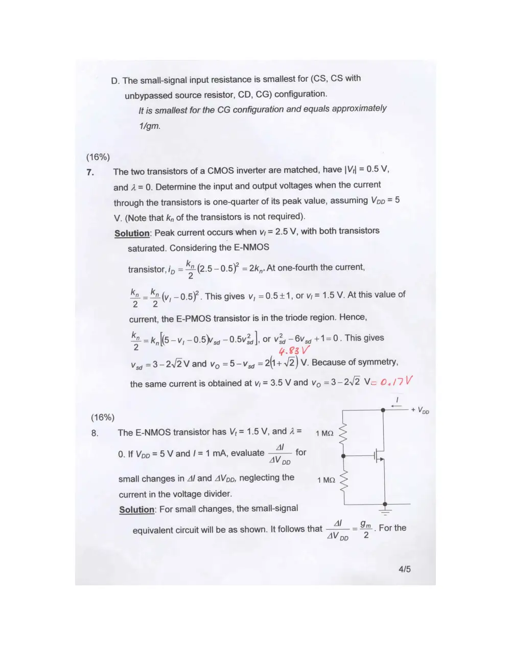
Te The two transistors of a CMOS inverter are matched, have |Vi| = 0.5 V,
and 4 = 0. Determine the input and output voltages when the current
through the transistors is one-quarter of its peak value, assuming Vpp = 5
V. (Note that k, of the transistors is not required).
Solution: Peak current occurs when v; = 2.5 V, with both transistors
saturated. Considering the E-NMOS
transistor, ip = Qs —0.5)° = 2k, At one-fourth the current,
Ky _ Kn
Sve tly -0.5). This gives v, =0.5+1, or v= 1.5 V. At this value of
2. woes
current, the E-PMOS transistor is in the triode region. Hence,
te = kl —v, —0.5Weq -0.5v3,|, or v2, —6V,q +1=0. This gives
Y83V
Veg =3-2V2V and Vo =5—Veq = 2(1+/2) V. Because of symmetry,
the same current is obtained at v, = 3.5 V and vp =3 EOD Ve Ons? V
|
—
(16%) + Vop
8. The E-NMOS transistor has V;=1.5V,and4= 4 Ma S
0. If Vpp = 5 V and / = 1 mA, evaluate for M
DD
small changes in Al and AVpp, neglecting the 4MQ
current in the voltage divider.
Solution: For small changes, the small-signal
equivalent circuit will be as shown. It follows that a
= 9m For the
DD 2
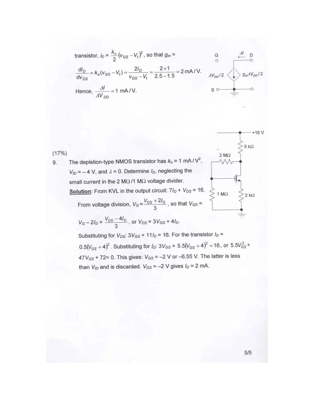
4/5
transistor, ip = “(Ves -V,)°, so that Om = G Alp
ie)
dip 2i 2x1
=k,(Ves —V;) = D___*“"__=2mA/V.
des nlVes -Vi) Ves -V; 2.5-1.5 AVpp!2 9nAVpp! 2
Hence, =1mA/V. Ss
DD =
———#— +16V
5kQ
(17%) i
; ; , 2MQ
9. The depletion-type NMOS transistor has k, = 1 mA/V*, = —AA/\-—#
Vip = -4 V, and 2 = 0. Determine /p, neglecting the
small current in the 2 MQ/1 MQ voltage divider. — —e
Solution: From KVL in the output circuit: 7/p + Vos = 16.
a 4MQ 2kQ
From voltage division, Ve=v0s+2o , so that Ves =
=
Ve —-2lp= “use or Vps = 3Ves + 41b.
Substituting for Vos: 3Ves + 11/p = 16. For the transistor Ip =
0.5(Veg +4). Substituting for Ip: 3Ves + 5.5(Ves +4) =16, or 5.5Vg5+
47 Ves + 72= 0. This gives: Ves = —2 V or 6.55 V. The latter is less
than Vip and is discarded. Ves = —2 V gives Ip = 2 mA.
5/5
6. Given an enhancement NMOS transistor having k’= 50 wA/V’, W= 100 um, and L = 10 um, V;= 1
V, with the gate connected to the drain. Determine the voltage across the device if the current is 4
mA
a)1V b)6V c)5V d3V e) none of the above
7. The two transistors of a CMOS inverter are matched, have k'(W/L) = 1 mA/V’, V=1V, Vp
being 4 V. At what input voltage is the current in the Vpp supply maximum?
a)2V b)4V 0)3V d6V e) none of the above
8. In the previous problem, determine the peak current in the Vpp supply, assuming zero load.
a) 5mA b)2mA c) 1 mA d)0.5mA e) none of the above
9. In the circuit shown on the right, Vpp = 5 V, Ipp = 1 mA, the two +¥ op
transistors are identical and have k’,(W/L) = 1 mA/V? and V,= 1 V. If V;=
2 V, determine Vo. I
DD
a)1V b)3V
c)2.5V d2V
e) none of the above +
—tE A Vo
ZF =
10. If the transistors in the preceding problem have 2 = 0.1 V"', determine the small-signal gain (v,/v,)
around the same DC operating point.
a)-10 b) -6.2 c) -2.6 d) +5 e) none of the above
11. Refer to the circuit shown on the right. Determine R so that e 45V
the DC output Vo = 2 V, assuming B to be very large,
Vee = 0.8 V, (W/L) = 0.2 mA/V*, and V,= 1 V. 2kKQ
1MQ
a) 4.36 MQ b) 3.17 MQ
c) 10.54 MQ d) 6.14 MQ
F +
e) none of the above Not applicable ir
go”
12. In the previous problem, find the collector current of the BJT. 2kQ
a)lS5mA b)05mA c)l.1mA_ d)2.1mA _
e) none of the above Not applicable
13. In the circuit shown on the right Q, and Q, are identical and have +Vinp
k’,(WIL) = 0.5 mA/V? and V,= 1 V, with Jp = 1 MA and Vpp = 10 V.
Determine Vps>. I
a)4V b)6V vy) ref
c)5V d)3V
e) none of the above a J
14. In the previous problem, find the value of Vps). Ly 22
a) 1.23 V b) 0.83 V
c)2.17V d) 2.85 V
e) none of the above Hy 1
15. In the circuit shown on the right, Rg = 30 kQ, Rp = 20 kQ, gy, 4V,
= 0.5 mA/ V, and r, = 80 kQ. Determine the midband gain v,/y,. re
a) -12.8 b) -8.6
c) -6.1 d) -4.9 Rp
e) none of the above Rg
=
+
16. In the preceding problem, if C = 50 uF, the corner frequency
in rad/sec is: C2 Mp
a)2.37 b)3.91_ ce) 18.6 ~— d) 4.87 ra | | b Vv,
e) none of the above :
Not applicable v;