
EECE 311 Lecture 3, Spring 2012
American University of Beirut · Electronic Circuits · 56 pages



Showing the first 10 of 56 pages. Download the PDF to see all of it.
More EECE 311 files
Show the text of this lab
EECE 311: Electronic Circuits
Part 3
2
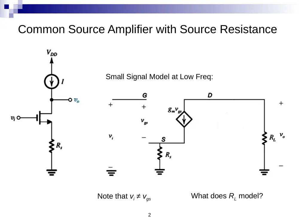
Common Source Amplifier with Source Resistance
Small Signal Model at Low Freq:
What does RL model?
Note that vi ≠ vgs
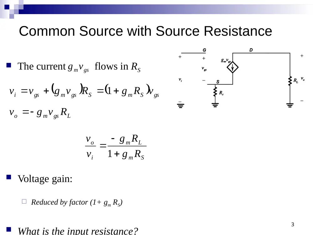
Common Source with Source Resistance
The current flows in RS
Voltage gain:
Reduced by factor (1+ gm RS)
What is the input resistance?
3
mvgs
g
S gs
m
S
gs
m
gs
i
v
g R
R
g v
v
v
1
L
gs
m
o
g v R
v
S
m
L
m
i
o
R
g
R
g
v
v
1
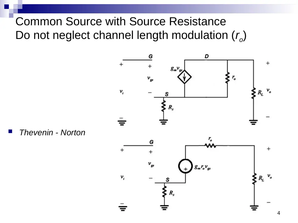
Common Source with Source Resistance
Do not neglect channel length modulation (ro)
Thevenin - Norton
4
Common Source with Source Resistance
Do not neglect ro
ro causes the gain to drop (further)
5
1
1
m o
gs
o
L
S
m o
L
gs
o
L
o
L
S
m o
S
i
gs
S
gs
o
L
S
o
m o
L
m
L
i
o
L
S
m o
S
L
S
m
S
o
g r v
i
r
R
R
g r R v
v
R i
r
R
R
g r R
v
v
R i
v
r
R
R
v
g r R
g R
v
r
R
R
g r R
R
R
g R
r
i
Common Source with Source Resistance
Do not neglect ro
What is the input resistance?
What is the output resistance?
6
Common Source with Source Resistance
Do not neglect ro
Output resistance?
7
Common Source with Source Resistance
Do not neglect ro
Output resistance
RXY = RX + RY + gm RX RY
Ro = ro + RS + gm ro RS
Looking into the drain of a MOSFET, with gate at DC (no
signal), and resistance RS between source and ground, a
resistance ro + RS + gmroRS is seen (from drain to
ground).
8
BJT Common-Emitter with RS
Small-Signal Equivalent Circuit
9
Input Resistance of CE with RS
Ri = vi / ii
vp = rp ii
vi = vp + Rs (ii + gm vp)
= rp ii + RS (ii + gm rp ii)
vi / ii = rp + RS (1 + gm rp)
But gm rp = b :
Ri = vi / ii = rp + (b + 1)RS
10
BJT Base Reflection Rule
The resistance seen looking into the base is:
rp + (b + 1) times the resistance between the
emitter and ground
…the resistance in the emitter appears (b +
1) times larger when looking into the base.
Fine print: The above rule applies when ro is very large (negligible Early Effect)
11
BJT Common-Emitter Small-Signal
Equivalent Circuit
Voltage gain:
Similar to MOSFET result
12
1
o
m
L
m
i
S
v
g R
g
v
R
BJT Common-Emitter with RS
Output Resistance
Hint: Recycle!
Output resistance:
use MOSFET result
after noting that
rp and RS are connected in parallel for the Ro
calculation (when vi is set to zero):
Ro = ro + (rp // RS) + gm ro (rp // RS)
13
14
Common-Gate Amplifier with Active Load
from S to D
appears
controlled source
a
circuit :
equivalent
that in the small - signal
Note
i
m
i
gs
g v
v
v
15
Input Resistance:
m
i
i
i
i
m
i
g
i
v
R
g v
i
1
Voltage gain:
L
m
m
i
i
L
i
o
v
L i
o
R
g
g
i
i
R
v
v
A
R i
v
Output resistance:
o
i
m
R
g v
0
Current gain:
1
i
i
o
A
i
i
Common-Gate Amplifier
Resistance Looking into
MOSFET Source Terminal
The resistance seen looking into the MOSFET
source with gate at DC levels (no signal) is equal
to 1/gm
Does NOT apply when ro is not neglected (not )
1/gm becomes an approximation
16
17
Input Resistance
Note
•
We calculated Rin and not Ri
•
Rin depends on RL
Common-Gate Amplifier (with ro)
1
1 //
when
0
1
i
o
i
m i
o
i
L i
o
L i
i
m i
o
i
o
L
in
i
m o
o
in
o
L
m o
m
v
v
i
g v
r
v
R i
v
R i
i
g v
r
v
r
R
R
i
g r
r
R
r
R
g r
g
18
0
0
L
L
i
R
i
i
Open-Circuit Voltage Gain
Voltage Gains (RL connected)
o
o
i
in
v
v
sig
i
sig
in
s
v
v
v
R
G
A
v
v
v
R
R
Note
•
Av , Gv are positive (non-
inverting)
o
i
L
v
i R
i
o
L
in
v
v
R R
L , which is also equal to
L
v
vo
in
L
o
R
R
A
A
R
R
r
i o
m
i
o
g v r
v
v
o
m
R
i
o
vo
g r
v
v
A
L
1
19
(by inspection)
o
o
R
r
Output Resistance
Rout = output resistance with vsig = 0
Common Gate Characteristics
Large Output Resistance
Small Input Resistance
Unity Current Gain
Good current buffer
Ro = output resistance with vi = 0
calculation:
XY
out
o
S
m o
S
R
R
r
R
g r R
20
Common-Gate at High Frequency (no ro)
1
Pole Frequency:
1
1
2
/ /
p
in
s
m
f
C
R
g
2
Pole Frequency:
1
2
p
out
L
f
C
R
1
2
1
1
o
m
sig
p
p
V
A
V
s
s
Node equation at S
(after Norton transformation):
sig
s
in
s
m
s
s
s
V
V
sC V
g V
R
R
1
o
m
L
s
out
L
V
g R
V
sC
R
1
1
s
sig
m
s
in
s
V
V
g R
sC R
Node equation at D:
o
out
o
m
s
L
V
sC V
g V
R
Note: body is grounded
21
Considering ro
by OCTC:
Resistance seen by
//
in
s
in
C
R
R
Note
•
No Miller (multiplication)
effect
•
Larger bandwidth than
Common-Source
1
2
//
//
H
in
s
in
out
out
L
f
C
R
R
C
R
R
Resistance seen by
//
out
out
L
C
R
R
22
Common-Base Amplifier
Small Signal Model:
23
/ /
(
/ /input resistance of the CG)
1
o
L
in
m o
r
R
R
r
r
g r
Input Resistance
•
very small input resistance
(
) when is very large (no Early Effect)
1
in
i
e
e
o
r
R
R
r
r
r
24
by inspection?
similar to MOSFET with
replaced by
/ /
/ /
/ /
o
o
out
s
e
out
o
e
m o
e
R
r
R
R
R
r
R
r
R
r
g r
R
r
Output Resistance
25
Cascode Amplifier
Common-Source + Common-Gate
26
Input Resistance:
by inspection
in
R
Output Resistance:
The last stage is a common-gate
CG
out
out
S
o
m o
S
CG
R
R
R
r
g r R
the signal source
resistance of the
common-gate
stage is the
output resistance
of the common-
source stage.
2
2
2
1
2
2
1
2
CS
CS
out
o
o
m
o
o
o
o
m
o
o
R
R
r
g
r R
r
r
g
r r
27
Voltage Gain
L
o
o
d
vo
i
d
i
R
v
v
v
A
v
v
v
Input resistance of CG is the load on the CS stage
It happens to be when the load of the CG is an open circuit
Open-Circuit Voltage Gain of Cascode
L
v
vo
L
o
R
A
A
R
R
Voltage Gain with Load Connected
1
1
//
CG
CG
vo
m
o
in
A
g
r
R
2
2
1
1
2
1
m
o
m
o
m o
g
r
g r
g r
28
Rsig
vsig
Q1
Q2
Cdb2
Cdb1
Cgs2+Csb2
Cgd2
Cgs1
Cgd1
CL
RL
Cascode High Frequency Response
29
Rsig
Q1
Q2
Cgs1
RL
Resistance seen by Cgs1
30
Rsig
Q1
Q2
Cdb1+Cgs2+Csb2
RL
Resistance seen by Cdb1+Cgs2+Csb2
31
Rsig
Q1
Q2
CL+Cgd2+Cdb2
RL
Resistance seen by CL+Cgd2+Cdb2
32
Rsig
Q1
Q2
Cgd1
RL
Resistance seen by Cgd1
33
1
1
2
2
2
2
1
*
2
1
2
2
1
2
2
1
2
*
*
1
OCTC:
//
//
//
=
1
//
//
gs
CS
CG
CS
db
gs
sb
L
gd
db
gd
C
sig
in
sig
o
L
in
o
o
C
C
C
m
o
L
out cascode
L
o
o
m
o
o
C
C
C
C
sig
m
sig
R
R
R
R
r
R
R
R
R
r
R
g
r
R
R
R
R
r
r
g
r r
R
R
R
g R R
1
1
1
2
2
2
*
XY
1
1
2
2
2
2
1
//
This is an R
1
CG
CS
gs
gd
db
gs
L
gd
db
in
o
H
gs
C
db
gs
sb
L
gd
db
gd
C
C
C
C
C
C
R
R
R
C
R
C
C
C
R
C
C
C
R
C
R
We use the results derived previously for
input and output resistances of common-
source and common-gate stages
34
Cascode Current Source
Large Output Resistance
Serves well as a current source
(load) for an amplifier
35
BJT Cascode
1
1
1
2
2
2
2
(
)
2
2
1
2
//
of CB when load is open circuit is
1
v
m
o
in
v
vo
vo CB
m
o
vo
v
vo
A
g
r
r
R
r
A
A
A
g
r
A
A
A
36
Open-Circuit Voltage Gain
Input Resistance by inspection
1
Rin
r
Output Resistance
'
'
'
1
2
2
2
2
1
//
1
(1
)
out
e
m
e
o
e
o
out
m
o
o
o
R
R
g R
r
R
r
r
r
R
r
g r
r
r
r
CB formula
37
Common Drain (Source Follower)
Small Signal Model:
38
Small-signal equivalent circuit:
Input Resistance
in
R
Voltage Gain
o
m
gs
L
v
g v R
Open-Circuit Voltage Gain
1
L
o
vo
i
R
v
A
v
i
gs
o
o
o
m
L
v
v
v
v
v
g R
1
o
m
L
v
i
m
L
v
g R
A
v
g R
39
Output Resistance
0
1 resistor appears from source to drain
1
i
gs
s
o
m
gs
m o
m
o
m
v
v
v
v
g v
g v
g
R
g
very small
CD used with low impedance load
Gain close to (but less than) one
output "follows" the input
Ro
40
Common Drain
with channel length modulation (ro)
Small Signal Model:
41
Equivalent Circuit:
Input Resistance
in
R
Voltage Gain
Open-Circuit Voltage Gain
1
1
L
o
m o
vo
i
m o
R
v
g r
A
v
g r
'
'
1
o
m
L
v
i
m
L
v
g R
A
v
g R
42
Output Resistance
1
/ /
o
o
m
R
r
g
43
Common Collector (Emitter Follower)
'
//
L
L
o
R
R
r
'
'
'
1
o
m
i
L
m
i
i
L
i
L
v
g v
i R
g r i
i R
i R
'
1
i
i
i
L
v
r i
i R
44
Input Resistance
'
1
i
in
L
i
v
R
r
R
i
Voltage Gain
'
'
1
1
L
o
v
i
L
R
v
A
v
r
R
Open Circuit Voltage Gain
1
o
vo
o
e
r
A
r
r
Large Input Resistance
Open Circuit Voltage Gain nearly
one: Signal at emitter “follows”
signal at input
45
Output Resistance
Very Low Output Resistance
1
or
i
x
i
i
i
1
o
x
r
o
i o
x o
v
i r
i r
i r
not included
/ /
1
1
sig
o
o
o
e
e
R
o
r
R
r
r
r
r
r
x
i
sig
v
i
r
R
1
1
x
o
out
o
x
sig
v
r
R
r
i
r
R
46
Some Useful Transistor Pairings
Common Collector – Common Emitter Pairing
larger than that of CE
1
CE
M
in
in
G
R
R
Wide Bandwidth
Large Input Resistance
47
Darlington Pair
1
2
Effective
High-Performance Voltage Follower
48
Common Drain – Common Gate Pairing
CD
CG
CG
vo
v
vo
vo
A
A
A
A
Infinite Input Resistance
Voltage gain ~ ½ CG
Very Good High Frequency
Response
1
49
Common Collector – Common Base Pairing
PNP Common-Base
Stage
Very Good High-
Frequency Performance
Improved Current Sources
Larger output resistance (current less
dependent on voltage – closer to ideal)
Less dependence on transistor
parameters (such as in BJT)
Without sacrificing voltage range?
Voltage across real current sources (VCS)
cannot drop below a certain minimum
50
51
Cascode MOS Mirror
Large output resistance
But reduced range of VO
min
3
4
2
2
since
2
2
O
t
ov
G
GS
GS
t
ov
v
V
V
V
V
V
V
V
52
Improved Bipolar Current Mirror
2
1
1
REF
C
I
I
Dependency on β decreased
from 1/ β to 1/ β2 (error term is β
times smaller)
But output resistance still the
same (ro2)
What about voltage range?
2
1
1
2 /
o
C
o
REF
I
I
I
I
2
2
1
1 2 /
1
2 /
53
Wilson Current Mirror
2
1
1
2
1
1
1
C
o
REF
C
I
I
I
I
Dependency on β decreased from
1/ β to 1/ β2
Output resistance multiplied by β/2
But reduced range of Vo (Vomin = 1V)
2
2
1
2
1
2
1
2
1
1
2 /
54
Wilson MOS Mirror
3
3
3
2
3
3
1
1
3
3
2
1
m
o
o
m
o
o
o
m
m
o
m
o
o
g
R
r
g
r r
r
g
g
R
g
r r
Large output resistance
But reduced range of VO
55
Improved Balanced Wilson MOS Mirror
Same as Wilson MOS current but
with balanced drain voltages of
Q1 and Q2.
56
Widlar Current Source
Can generate a small constant
current using relatively small
resistors.
1
2
2
BE
BE
E
E
V
V
I
R
Output Resistance
1
//
o
m
E
o
R
g
R
r
r
1
2
2
ln
1
ln
1
C
C
T
T
E
E
S
S
I
I
V
V
I
R
I
I