
EECE 311 Lecture 5, Spring 2012
American University of Beirut · Electronic Circuits · 35 pages
Showing the first 10 of 35 pages. Download the PDF to see all of it.
More EECE 311 files
Show the text of this lab
EECE 311: Electronic Circuits
Part 5
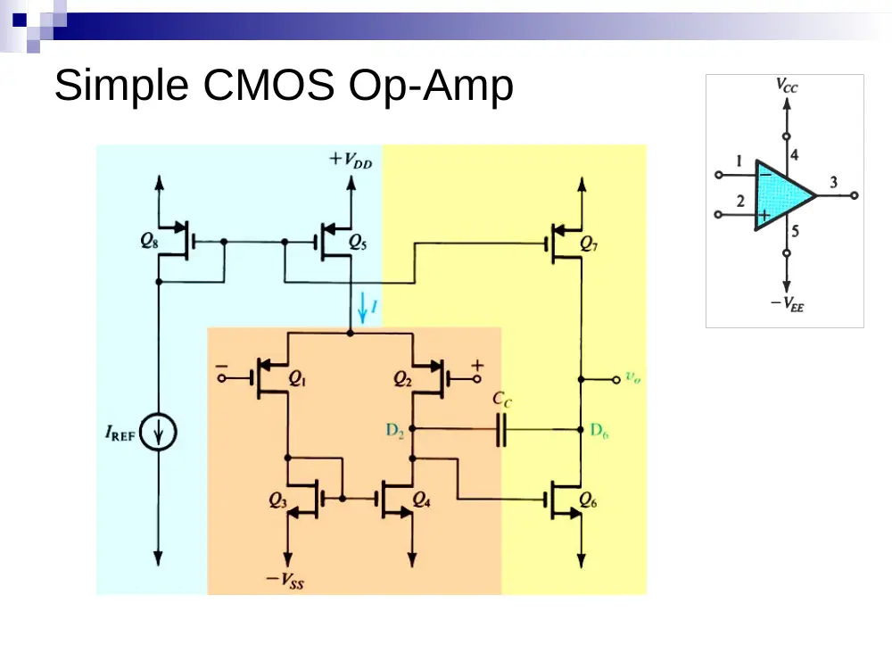
Simple CMOS Op-Amp
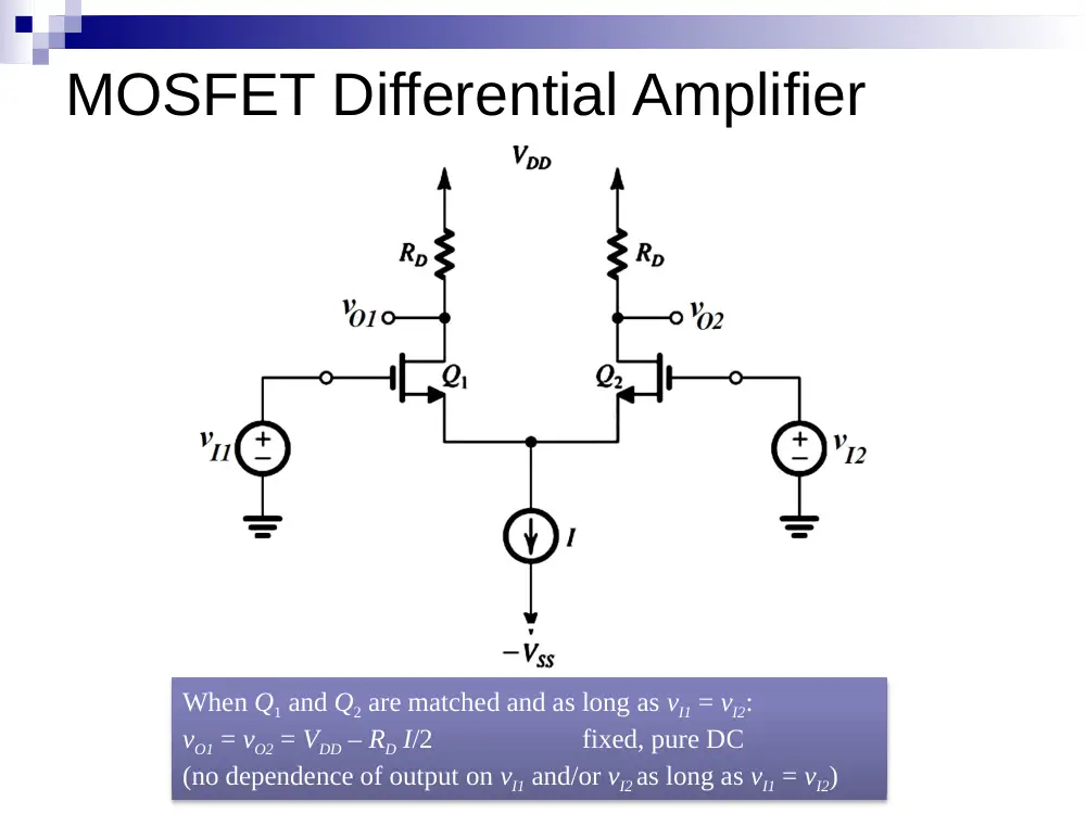
MOSFET Differential Amplifier
When Q1 and Q2 are matched and as long as vI1 = vI2:
vO1 = vO2 = VDD – RD I/2 fixed, pure DC
(no dependence of output on vI1 and/or vI2 as long as vI1 = vI2)
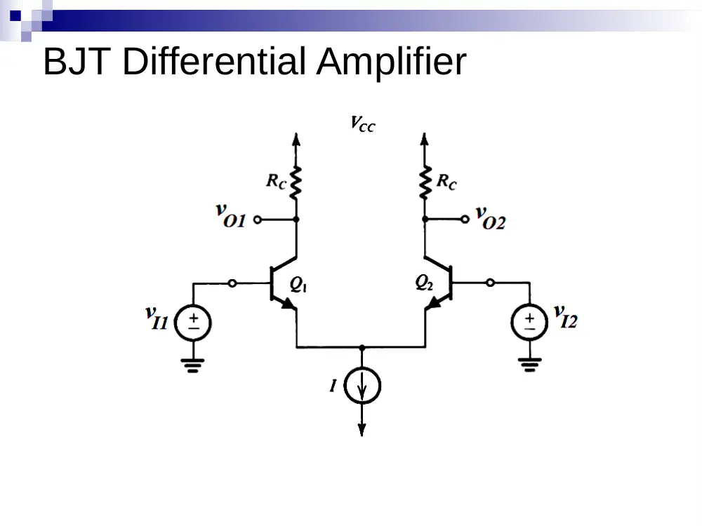
BJT Differential Amplifier
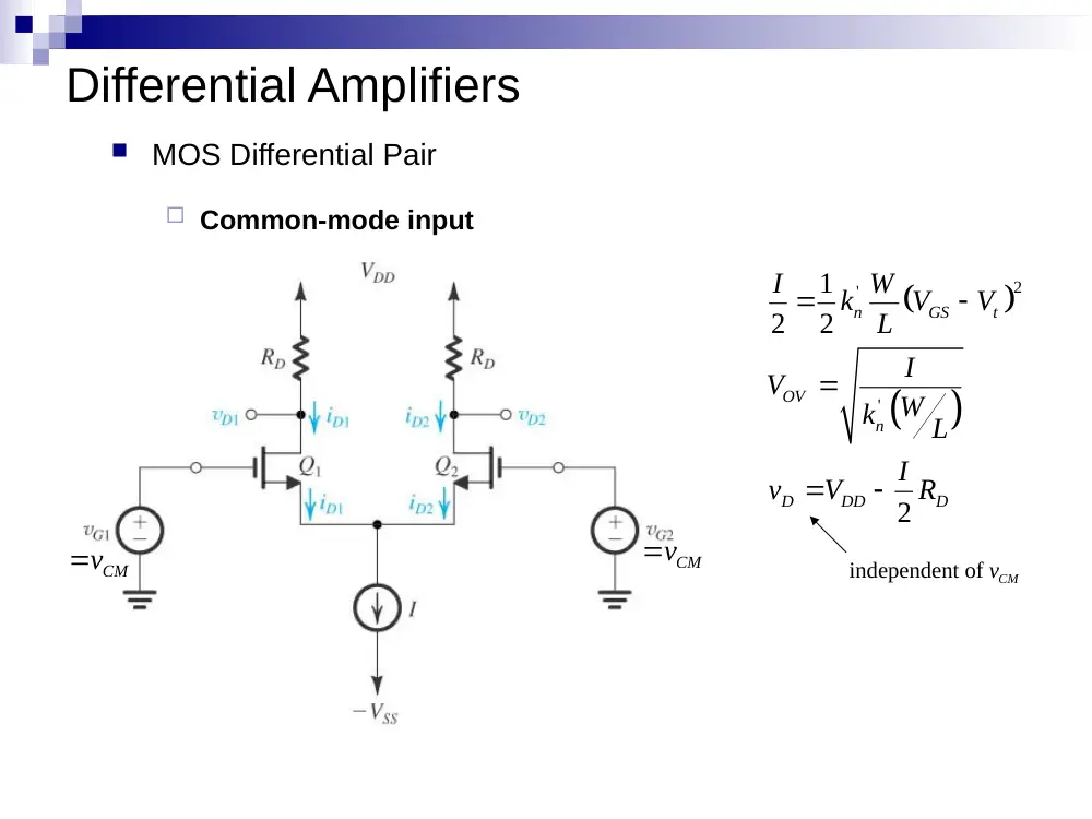
Differential Amplifiers
MOS Differential Pair
Common-mode input
2
'
'
1
2
2
2
n
GS
t
OV
n
D
DD
D
I
k W
V
V
L
I
V
W
k
L
I
v
V
R
vCM
vCM
independent of CM
v
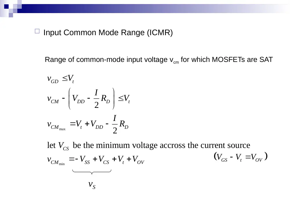
Input Common Mode Range (ICMR)
min
let
be the minimum voltage accross the current source
CS
CM
SS
CS
t
OV
V
v
V
V
V
V
Sv
GS
t
OV
V
V
V
max
1
2
Range of
for which
and
are SAT
2
2
CM
GD
t
CM
DD
D
t
CM
t
DD
D
v
Q
Q
v
V
I
v
V
R
V
I
v
V
V
R
Range of common-mode input voltage vcm for which MOSFETs are SAT
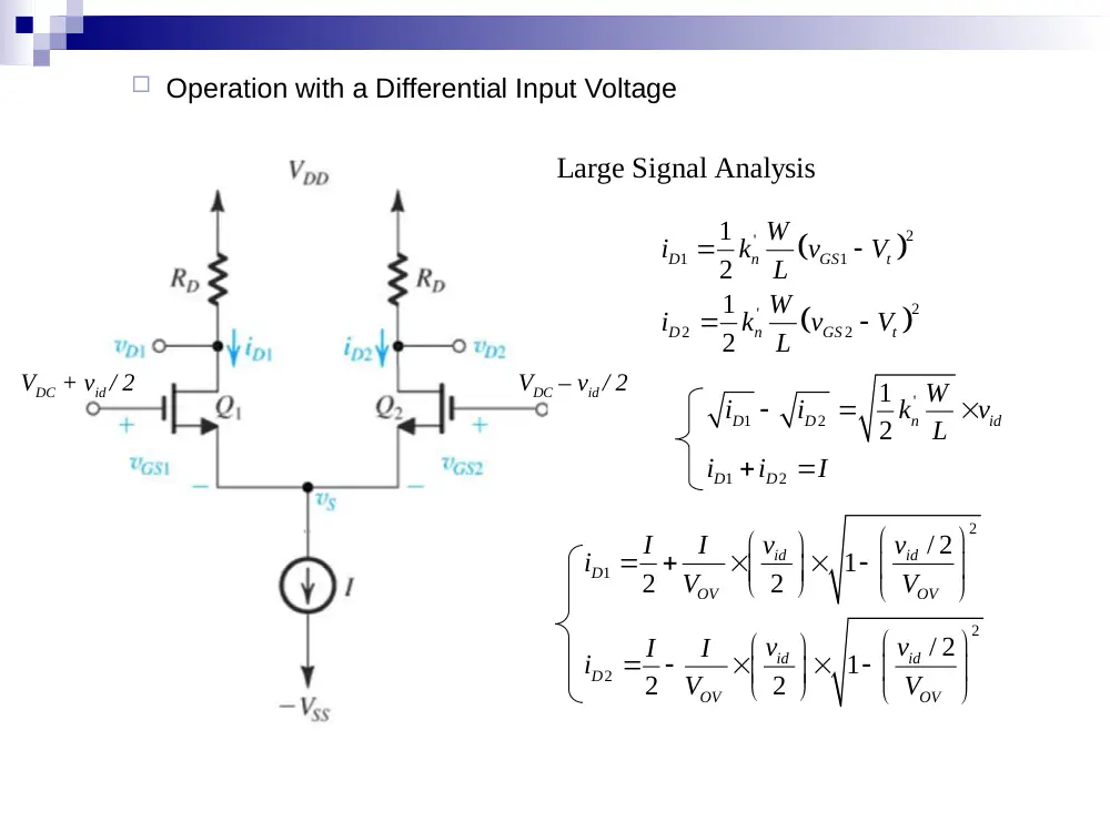
Operation with a Differential Input Voltage
2
'
1
1
2
'
2
2
1
2
1
2
D
n
GS
t
D
n
GS
t
W
i
k
v
V
L
W
i
k
v
V
L
Large Signal Analysis
'
1
2
1
2
1
2
D
D
n
id
D
D
W
i
i
k
v
L
i
i
I
2
1
2
2
/ 2
1
2
2
/ 2
1
2
2
id
id
D
OV
OV
id
id
D
OV
OV
v
v
I
I
i
V
V
v
v
I
I
i
V
V
VDC – vid / 2
VDC + vid / 2
1
if
:
ID
I
2
2
/ 2
/ 2
/ 2
1
1
1
let
2
1
1
2
2
id
id
id
OV
OV
OV
id
OV
v
v
v
x
V
V
V
x
x
v
V
/ 2 2
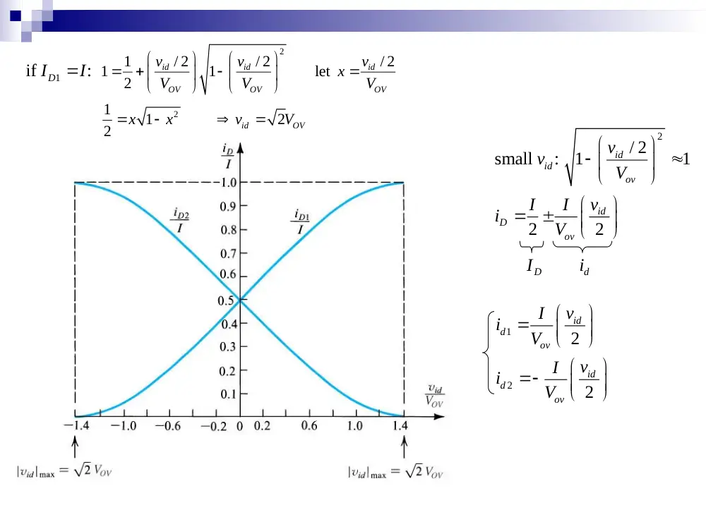
small
: 1
1
2
2
id
id
ov
id
D
ov
v
v
V
v
I
I
i
V
ID
di
1
2
2
2
id
d
ov
id
d
ov
v
I
i
V
v
I
i
V
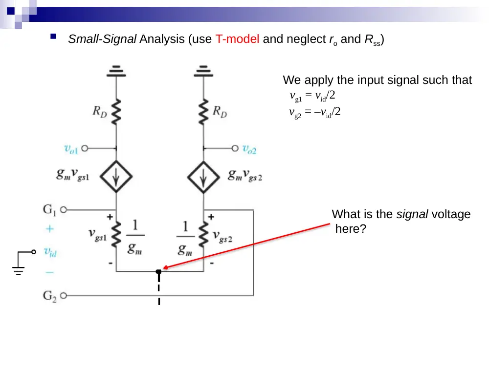
Small-Signal Analysis (use T-model and neglect ro and Rss)
What is the signal voltage
here?
We apply the input signal such that
vg1 = vid/2
vg2 = –vid/2
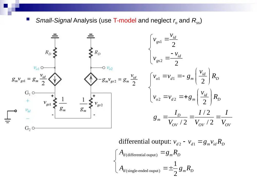
Small-Signal Analysis (use T-model and neglect ro and Rss)
1
2
2
2
id
gs
id
gs
v
v
v
v
2
1
(differential ouput)
(single-ended ouput)
differential output:
1
2
d
d
m id
D
d
m
D
d
m
D
v
v
g v R
A
g R
A
g R
1
1
2
2
2
2
/ 2
/ 2
/ 2
id
o
d
m
D
id
o
d
m
D
D
m
OV
OV
OV
v
v
v
g
R
v
v
v
g
R
I
I
I
g
V
V
V
Small-Signal Analysis (considering ro and Rss)
considering the output resistance
of the current source (Rss):
→ no difference since vs = 0 for
differential inputs
considering ro:
→ simply replace RD by RD// ro
(for the same reason)
Half-circuit concept
Since vs = 0 when inputs are applied differentially
'
1
1
2
1
/ /
2
o
m
L
id
o
m
o
D
id
v
g R
v
v
g
r
R
v
MOSFET biased at I/2
What kind of circuit is the half circuit?
Common-Mode Gain & CMRR
Use the half-circuit concept
What kind of circuit is the half circuit?
1
2
1
2
2
2
o
D
D
cm
SS
SS
m
o
D
cm
SS
v
R
R
v
R
R
g
v
R
v
R
Differential Output
2
1
0
o
o
cm
icm
v
v
A
v
CMRR
Single-Ended Output
2
1
2
2
o
D
cm
icm
SS
m
D
SS
d
m
SS
cm
D
v
R
A
v
R
g R
R
A
CMRR
g R
A
R
MOSFET Differential Amplifier
CMOS implementation
How do we generate
VBIAS1 and VBIAS2?
What is the voltage gain?
MOSFET Differential Amplifier
CMOS Cascode implementation
What is the voltage gain?
17
BJT Differential Pair
1
2
1
2
1
2
1
2
1
2
BE
T
BE
T
BE
T
BE
T
v
V
C
S
v
V
C
S
v
V
S
E
v
V
S
E
E
E
i
I e
i
I e
v
I
i
e
I
i
e
i
i
I
18
1
2
1
2
1
2
1
2
1
1
1
1
B
B
T
B
B
T
id
T
id
T
E
v
v
V
E
v
v
V
C
v
V
C
v
V
I
i
e
I
i
e
I
i
e
I
i
e
-10 mV< vid < 10 mV
19
Solution to small vid range:
Introduce a resistance in the emitter to trade gain for increasing linearity
20
BJT Differential Pair Small Signal Analysis
1
1
1
2
2
1
id
id
e
b
e
e
e
v
v
v
i
i
r
r
r
Small-signal equivalent circuit using T-model
with Re=0
21
Differential Input Resistance
1
1
2
1
2
with
:
2
1
id
id
e
b
e
id
id
e
e
b
v
R
r
r
i
R
v
R
r
R
i
Differential Voltage Gain
1
1
1
2
2
1
2
1
2
with
:
id
c
m
C
m
C
c
m
C
id
c
m
C
id
e
C
d
e
e
v
v
g v R
g
R
v
g R
v
v
g R
v
R
R
A
R
r
1
2
c
c
d
m
C
id
v
v
A
g R
v
Even with a non-ideal current source (with finite
output REE), the emitter voltage will still be zero
because of symmetry and nothing will change in
the previous analysis.
22
Common-Mode Gain
Half-circuit:
1
2
2
2
0
2
1
2
2
c
c
C
C
icm
icm
EE
e
EE
cm
C
cm
EE
m
C
m
EE
C
EE
v
v
R
R
v
v
R
r
R
A
CMRR
R
A
R
g R
CMRR
g R
R
R
(differential output)
(single-ended output)
Bipolar Differential Amplifier
NPN-PNP implementation
How is the current source
implemented?
What is the voltage gain?
24
The MOS Differential Amplifier with Active Load
Current Mirror
Could use Wilson Current Source
Differential Pair
Could be cascoded to increase output
resistances in parallel with the active loads
Current Sink
Could be cascoded to increase Rss
25
Differential Input: Small-Signal Analysis
Determining Ro and Gm
1
2
2
4
2
4
Finding
by short-circuiting the output
to ground:
/ /
/ /
m
o
m
id
m
m
m
m
o
o
o
vo
m
o
m
o
o
G
i
G
v
G
g
g
g
R
r
r
A
G R
g
r
r
Twice the gain obtained from previous differential amplifier
Due to current mirror action
26
Common Mode Gain of MOS Differential Amplifier with Active Load
4
3
3
3
1
2
4
3
1
2
1
1
2
(
/ /
) 2
o
o
cm
icm
SS
m
o
cm
m
SS
m
o
o
m
SS
v
r
A
v
R
g
r
A
g
R
CMRR
g
r
r
g
R
27
BJT Active-Loaded Differential Amplifier
1
2
2
4
(
)
/ /
/ /
/ /
m
m
m
m
o
o
o
oN
oP
vo
m
o
m
oN
oP
G
g
g
g
R
r
r
r
r
A
G R
g
r
r
Similar results to the MOSFET circuit
4
3
3
1
2
o
cm
EE
m
EE
r
A
R
CMRR
g R
28
Frequency Response of the MOS Differential Amplifier
Differential Gain
Half-circuit is a CS amplifier
29
Frequency Response of the Resistively Loaded MOS Amplifier
Common-Mode Gain
1
1/
1/
o
D
m
gs
m
gs
icm
m
SS
v
R
g v
g
v
v
g
Z
neglecting and the capacitors
at input and output:
or
30
1
1/
1/
1/
1
2
1
where
2
// 2
1 2
2
1
1
2
1
2
1
1
1
/
1
2
1
/
o
m
m
D
D
D
m
icm
m
SS
m
SS
m
SS
SS
SS
SS
SS
SS
SS
SS
SS
m
D
SS
SS
m
D
cm
SS
m
SS
SS
SS
m
SS
SS
m
D
z
cm
m
SS
p
v
g
g R
R
R g
v
g
Z
g
Z
g Z
C
R
Z
R
R
sC
sR C
g R
sR C
g R
A
R
g R
sR C
g
sR C
g R
s
A
g R
s
1
1
2
z
SS
SS
m
SS
p
SS
SS
R C
g R
R C
pole >> zero
zero at a very low frequency
31
We try to make ωz higher so that the high
frequencies we are interested in would lie
in the domain where Acm is minimum and
not increasing (i.e. CMRR very large).
We do that by changing the size of the
MOSFETs.
32
Multistage Amplifiers
Simple CMOS Op-Amp
Current Mirror
Active-Loaded CS amplifier
Active-Loaded Differential Amplifier
33
Input Stage: Differential Amplifier
1
1
2
4
//
m
o
o
A
g
r
r
Second Stage: Common-Source Amplifier
2
6
6
7
//
m
o
o
A
g
r
r
1
6
2
4
6
7
//
//
o
d
m
m
o
o
o
o
id
v
A
g g
r
r
r
r
v
34
Frequency Response of the two-stage CMOS Op-Amp
2
2
1
1
2
2
1
6
2
2
2
2
2
node equation at D :
0
node equation at D :
0
i
m
id
i
C
i
o
o
m
i
o
C
o
i
V
G V
sCV
sC
V
V
R
V
G V
sC V
sC
V
V
R
1
2
1
1
1
z
o
id
p
p
s
K
V
V
s
s
35
1
2
1
1
2
2
2
2
2
2
is
much larger than
and
to stabilize the circuit
1
C
p
C
m
m
p
m
z
C
C
made
C
C
R C G
R
G
C
G
C
dominant pole
1
1
2
2
1
1
2
should be <
,
for stability
t
H
m
m
p
m
t
C
t
p
z
K
G R G
R
G
C