
EECE 311 Lecture, Spring 2012
American University of Beirut · Electronic Circuits · 7 pages



More EECE 311 files
Show the text of this lab
1
CMOS Common Source Amplifier
Based on input voltage vI, vo follows the voltage transfer characteristics
curve
Region III is the high gain region: Q1 and Q2 are in saturation
VIA < vI <VIB
VOB < vo <VOA
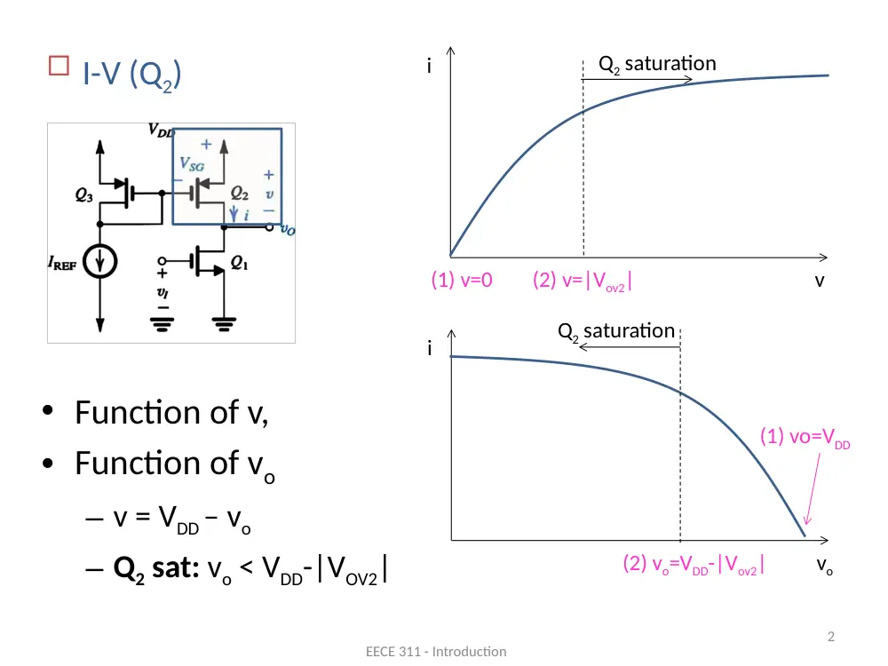
• Function of v,
• Function of vo
– v = VDD – vo
– Q2 sat: vo < VDD-|VOV2|
EECE 311 - Introduction
2
I-V (Q2)
v
i
(1) v=0
(2) v=|Vov2|
vo
i
(1) vo=VDD
(2) vo=VDD-|Vov2|
Q2 saturation
Q2 saturation
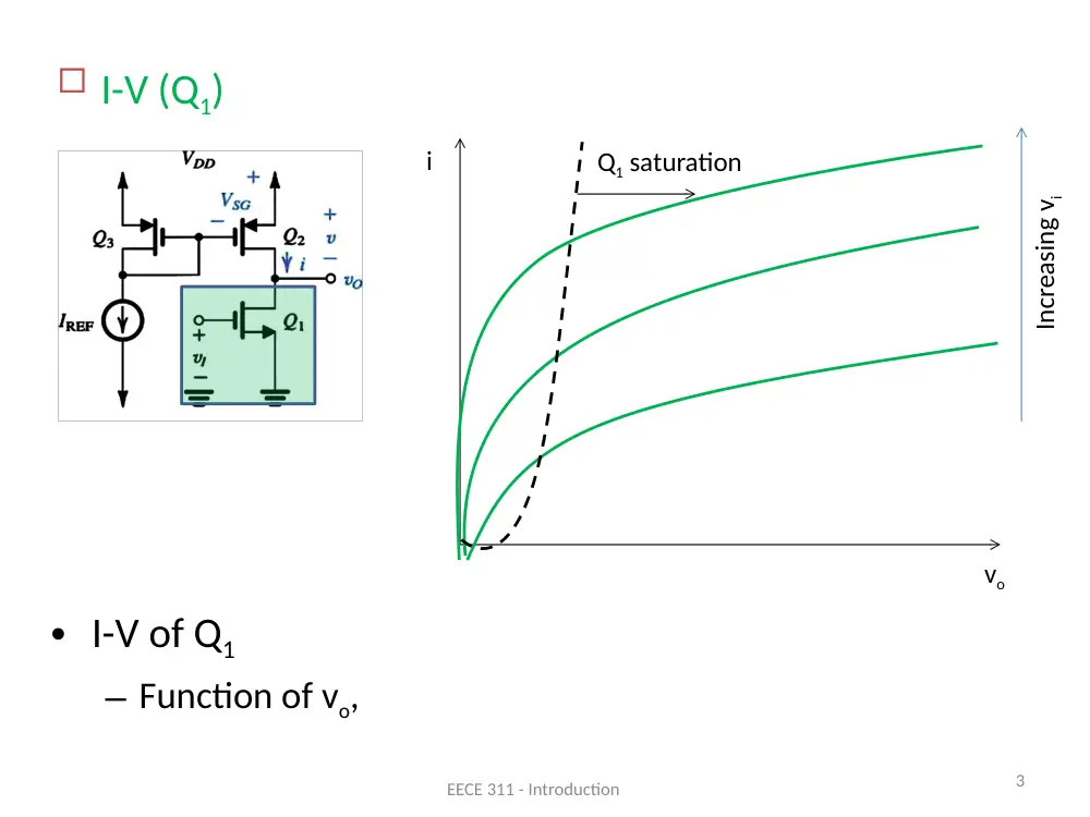
• I-V of Q1
– Function of vo,
EECE 311 - Introduction
3
I-V (Q1)
vo
i
Q1 saturation
Increasing vi
•
Intersection of
– I-V(Q1)
– I-V(Q2)
provides the solution space
EECE 311 - Introduction
4
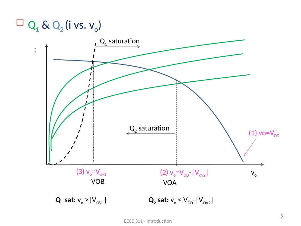
Q1 & Q2 (i vs. vo)
vo
i
(1) vo=VDD
(2) vo=VDD-|Vov2|
Q2 saturation
vo
i
Q1 saturation
EECE 311 - Introduction
5
Q1 & Q2 (i vs. vo)
vo
(1) vo=VDD
(2) vo=VDD-|Vov2|
Q2 saturation
i
Q1 saturation
(3) vo=Vov1
VOA
VOB
Q2 sat: vo < VDD-|VOV2|
Q1 sat: vo >|VOV1|
EECE 311 - Introduction
6
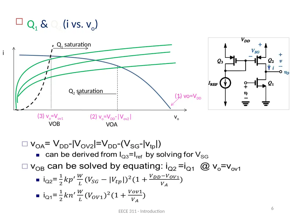
Q1 & Q2 (i vs. vo)
vo
(1) vo=VDD
(2) vo=VDD-|Vov2|
Q2 saturation
i
Q1 saturation
(3) vo=Vov1
VOA
VOB
•
1
2
'
2
2
1
1
1
1
1
2
2
1
1
1
1
1
2
1
1
2
2
1
2
100 A
100 A
200 (10)
0.316V
100
0.633 mA/V
0.5 0.316V
20
200K
100
10
100K
100
Output resistance:
//
66.67K
Voltage gain:
D
D
REF
W
D
n
OV
OV
L
OV
D
m
OV
An
o
D
Ap
o
D
o
o
o
I
I
I
I
k
V
V
V
I
g
V
V
r
I
V
r
I
R
r
r
1
1
2
2
2
'
1
1
2
2
2
2
2
1
//
42.2 V/V
Limits of output voltage swing:
100 A
65 (10)
0.6
1.155V
1.155
0.6
0.555V
enters SAT when:
3
0.555
2.445 V
enters SAT when:
v
m
o
o
W
REF
p
SG
tp
SG
L
SG
OV
O
DD
OV
O
A
g
r
r
I
k
V
V
V
V
V
Q
v
V
V
Q
v
1
0.316 V
VOV
7
Solution:
We will neglect channel-
length modulation in
DC analyses.
(i.e., when we solve for ID, VOV)
When we solve for small signal
parameters we will consider those
effects