
CSI 312 Final, Fall 2011
American University of Science and Technology · Computer Architecture · 4 pages · Dr. Abbas Tarhini
More CSI 312 files
Show the text of this final exam
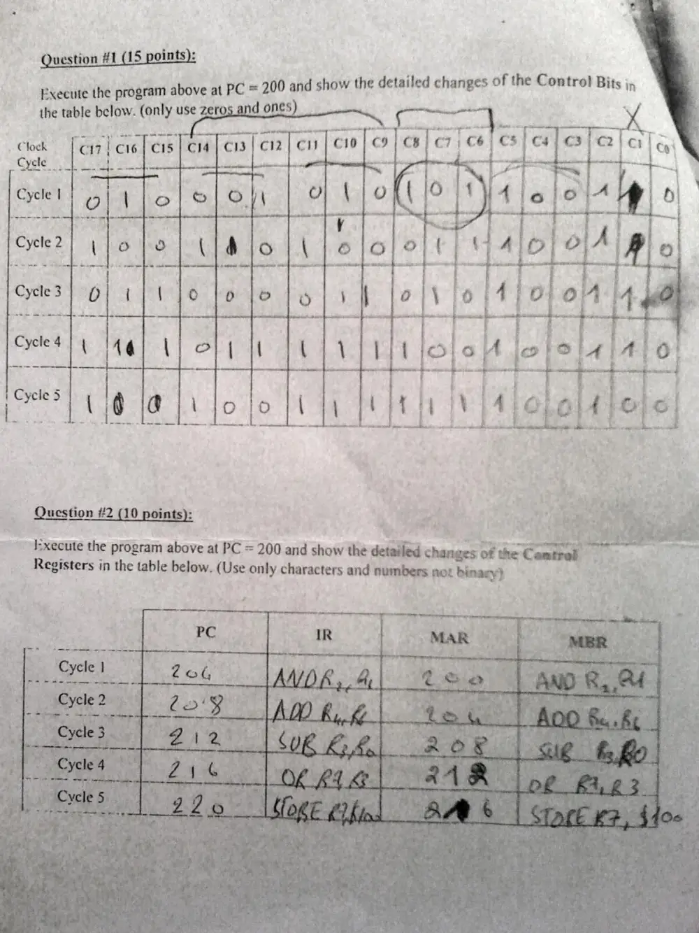
uestion #1 (15 points): i
above at PC = 200 and show the detailed changes of the Contro} Bits jp,
gram
Execute the pro
the table below. (only use zeros and ones
— pee
at ogee
ciolcolesl}e7) ce) es
Question #2 (10 points): + Hike. vie et id
I:xecute the program above at PC = 200 and show the detailed changes of the C
Registers in the table below, (Use only characters and numbers not binary}
4
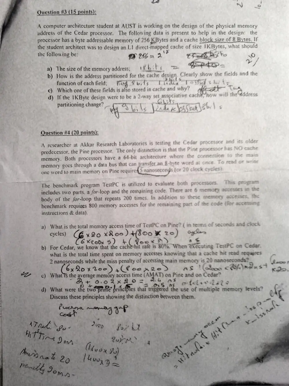
A computer architecture student at AUST is working on the desi i
oS, be: sign of the physical memor
address of the Cedar processor. The following data is present to help in the design: he
rocessor has a byte addressable memory of 256 KBytes and a cache block size of 8 Bytes. If
the student architect was to design an.L! direct-mapped cache of size | KBytes, what should
t ig aie es: FUG = 2? yo Yo sO
“ae = > = OF
a) Thesize of the memory address; bibs
__b) How is the address partitioned for the cache design. Clearly show the fields and the
———_ finetion of each field; ag Fests 1 a Ts al * kei
© Which one of these fields is also stored in cache and why? Lope
d+) Ifthe IKByte design were to be a 2-way set “ic Sake cach¥vhow will thedddress
partitioning change? -- pT 5. ene aa
| bg as Seed spent «
te ‘A researcher at Akkar Research Laboratories is testing the Cedar processor 2
___ predecessor. the Pine processor. The only distinction is that the Pine processor has WO cache
x memory. Both processors have a 64-bit architecture where the connection the mma
memory goes through a data bus that can transfer.an 8-byte word a
one word to main memon on Pine required nanosecongs (or 20 clack cycles}
7 ‘
nee > (eae
¢ benchmark program TestPC is utilized to evaluate both processors. “Thes program
Judes two parts. a for-loop and the remaining code, There are 6 memory accesses m the
-of the for-loop that repeats 200 times, In addition to these memory accesses, thre
ark requires 800 memory accesses for the remaining part of the code (fer accessing
structions & data).
“What is the
Hy} ye
total memory access time of TestPC on Pine? ( im terms of seconds amd clock
BX 20 XRoo)4{800 K 20) o>
®
th eEuting TestPC on Cedar
on memory accesses knowing that a cache hit read sequyres
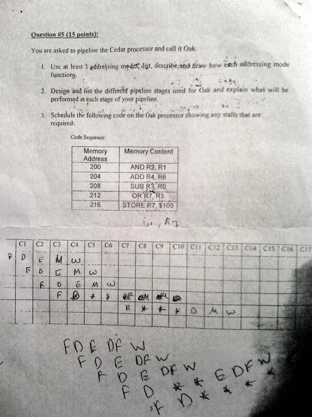
Question #5 (15 points):
You are asked to pipeline the Cedar processor and call it Oak:
’
1. Use at least 3 addressing modes, slipt, describe-and traw how each addressing mode
functions,
’
; . ‘ *% Lathe
af
-
2. Design and {ist the different pipeline stages used for Oak and explain what will be
performed at each stage of your pipeline.
4, 4 $ “ “s 94
Hiss 2 we Jas We 4
3. Schedule the following code on the Oak processor showing any stalls that are
required:
Code Sequence:
Memory Content
~~ AND R2,R1
ADD R4,R6 |
OR R?, 87, RS
“STORE R7, $1 x7, $100
ones eal [ Ci2 Cas Che] Cts C86 7
oy (ett MUR ieee ee te
ame i
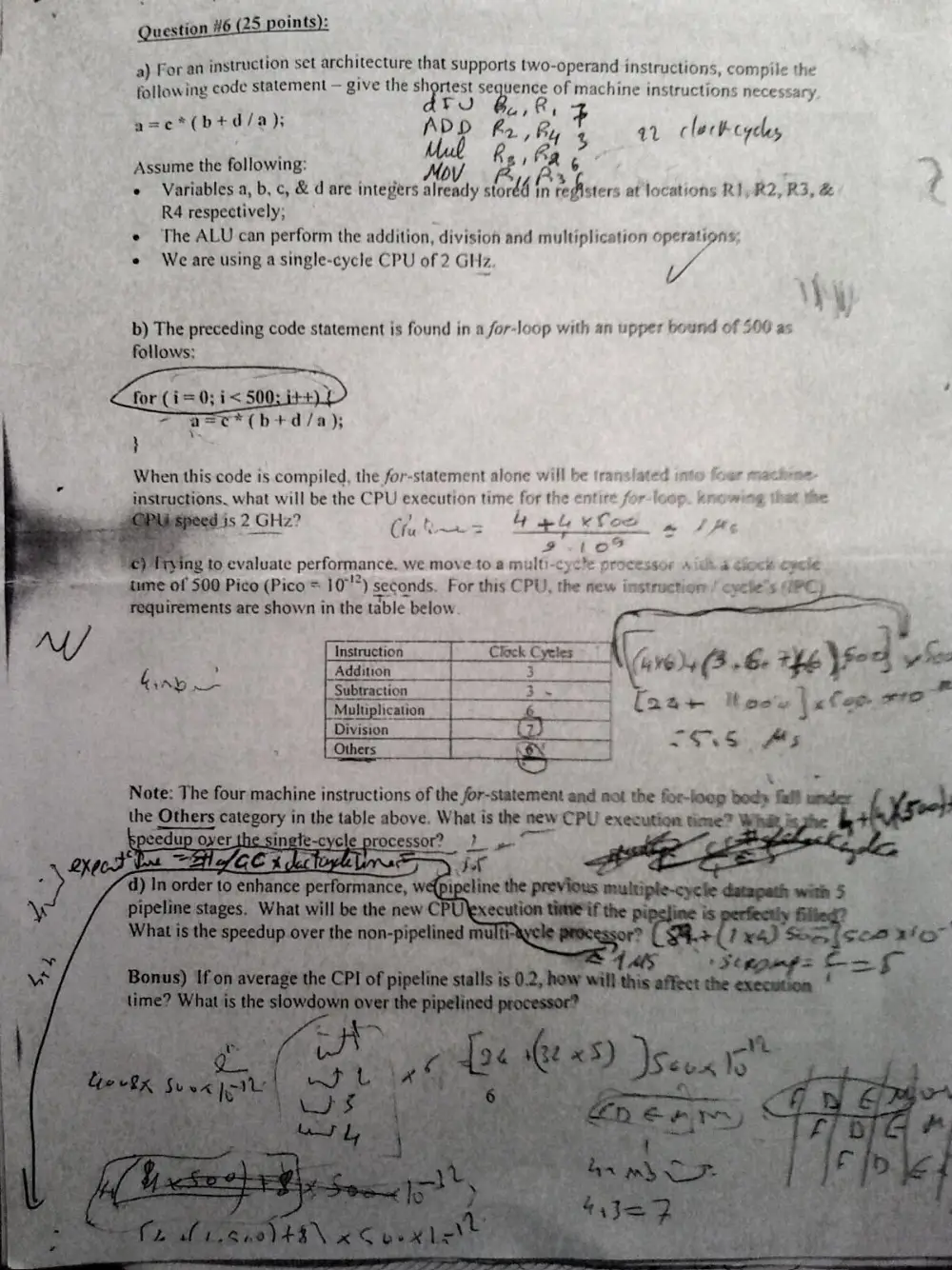
. Question #6 (25 points):
a) Foran instruction set architecture that supports two-operand instructions , compile the
following code statement — give the sh oe sequence of machine instructions necessary
Ri
Se ote bah ely Aon j. By q 41 clock cacles
Assume the following: Mad Be ‘Ba yn ‘
e Variables a, b, c, & d are integers 4 ee storéd in A> hover at locations RI, R2, R3, &
R4 respectively; ;
e¢ The ALU can perform the addition, division and multiplication operations,
We are using a single-cycle CPU of 2 GHz. nf
\ \ \,
b) The preceding code statement is found in a for-loop with an upper bound of 500 as
follows:
~
When this code is compiled, the for-statement alone will be translated into foer mactene
structions. what will be the CPU execution time for the entire for loop. knowmng thet the
2GHz? Bobs ate 5 a SMe
2 to evaluate perfomance. we move to a wines ao processor sith.d ciocis cycie
Multiplication
Piss: tons of hs sates onde Roe Do Bh
th egory in th es ee ee i