
CMPS 255 Final, Fall 2001
American University of Beirut · Computer Architecture · 7 pages



More CMPS 255 files
Show the text of this final exam
AMERICAN VNIVERSITA
LIBRARY
OF BEIBET
American University of Beirut
Math 255 Final Exam
Computer Architecture
Exam duration: 2 hour
AMERICAN UNTCERSITY
LIBRARY
OF BESRU'?
Name:
Student number:
Section: ase po | £00 2
Notes:
a. Students must put this question sheet inside the answer booklet.
b. Students must use ink, however they may use pencil and ruler for drawings.
c. Students have 10 minutes reading time.
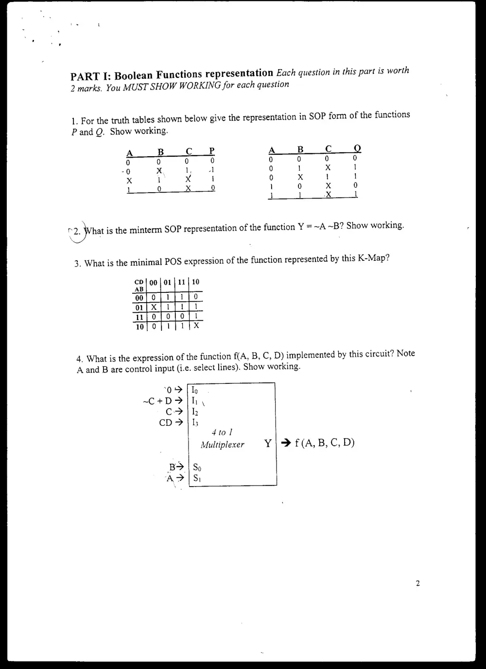
PART I: Boolean Functions representation Each question in this part is worth
2 marks. You MUST SHOW WORKING for each question
1. For the truth tables shown below give the representation in SOP form of the functions
P and Q. Show working.
B
0
x,
1
i}
£2. Wha is the minterm SOP representation of the function Y = ~A ~B? Show working.
3. What is the minimal POS expression of the function represented by this K-Map?
cp | 00} 01 | 11} 10
AB
00 1
01 1
ll Q
10 1
1 | 0
1{1
0 {1
1 {|X
4, What is the expression of the function f(A, B, C, D) implemented by this circuit? Note
A and B are control input (ie. select lines). Show working.
“00>
~C+D?
co
cD?
4tol
Multiplexer Y| => £(A,B, C, D)
So
Si
5. Give the expressions for the functions RX and S implemented by the following circuits.
Note B is the control input (i.e. the select line).
A?
~A? 2tol
B> Multiplexer
2tol
Multiplexer
PART I (15 marks): Each question in this part is worth 1 mark. DO NOT SHOW
WORKING.
1. A flip flop is:
_ A device that flips its output all the time.”
. A device that can store one bit.
. A device that can access the memory.
_ A device that can have three different output states. ,
Which one of the following is not true:
/X(Y+Z)=XY+XZ
_=X-V+XY=1
_X~X=0
| (X + YZ) = (X+Y) (X+Z)
A Moore sequential circuit is a circuit:
. With more output than input.
. With output depending on no more than 2 previous inputs.
. With output depending only on the present state.
. With output depending on the present state and the current input.
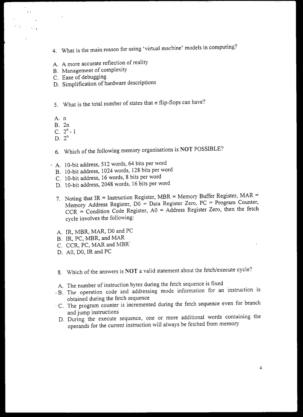
What is the main reason for using ‘virtual machine’ models in computing?
_ Amore accurate reflection of reality
_ Management of complexity
. Ease of debugging
. Simplification of hardware descriptions
What is the total number of states that ” flip-flops can have?
_ Which of the following memory organisations is NOT POSSIBLE?
- 10-bit address, $12 words, 64 bits per word
_ 10-bit address, 1024 words, 128 bits per word
_ 10-bit address, 16 words, 8 bits per word
_ 10-bit address, 2048 words, 16 bits per word
. Noting that IR = Instruction Register, MBR = Memory Buffer Register, MAR =
Memory Address Register, DO = Data Register Zero, PC = Program Counter,
CCR = Condition Code Register, AO = Address Register Zero, then the fetch
cycle involves the following:
_ IR, MBR, MAR, DO and PC
_ IR, PC, MBR, and MAR
. CCR, PC, MAR and MBR’
. AO, DO, IR and PC
Which of the answers is NOT a valid statement about the fetch/execute cycle?
_ The number of instruction bytes during the fetch sequence is fixed
. The operation code and addressing mode information for an instruction is
obtained during the fetch sequence
. The program counter is incremented during the fetch sequence even for branch
and jump instructions
. During the execute sequence, one or more additional words containing the
operands for the current instruction will always be fetched from memory
9. To convert serial data to parallel and parallel data to serial, the type of register
that is needed is:
A universal shift register
A parallel load register
A serial input register
A data register
OOw>
10. The storage capacity for a 256k x 64 memory chip is:
1 Mbyte
2 Mbyte
4 Mbyte
512 Kbyte
GOW,
11. MOVE R1,#5 (Where R1 is a CPU register) for a Pentium CPU is a:
Direct addressing instruction
Immediate addressing type instruction
Stack addressing type instruction
. Register addressing type instruction
cOw>
12. The number of address bits needed in a 2 byte words addressable machine with
2048 bytes is:
a 2-bit address
an 11-bit address
a 10 bit address
None of the above
VOWS
13. An appropriate combinational circuit that can be used to read a bit at a time from
a serial line and convert it to a byte is
Multiplexer
Decoder
Demultiplexer
None of the above
DOWD
14. Write -2789 in binary using 2’s complement representation:
—
15. Write 111010101111 in decimal:
Part III: Sequential circuits design (12 marks).
Question 1:
a. Use clocked D flip-flops to design a 3-bit counter which counts in the sequence:
001, 011, 010, 110, 111, 101, 100, 001, ...
b. A Moore sequential network has one input and one output. When the input
sequence 011 occurs, the output becomes | and remains | until the sequence 011
occurs again in which case the output returns to 0. The output then remains 0 until
011 occurs a third time, etc .
For example the input sequence: X= 01011 010110100111
Produces the output: Z=00001111100000011
Derive the state graph (Hint: 6 states should be enough).
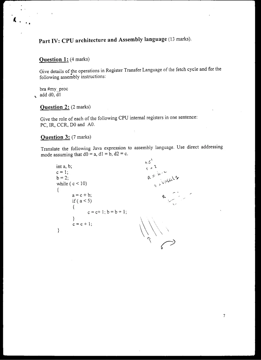
Part IV: CPU architecture and Assembly language (13 marks).
Question 1: (4 marks)
Give details of the operations in Register Transfer Language of the fetch cycle and for the
following assembly instructions:
bra #my - proc
add dO, dl
Question 2: (2 marks)
Give the role of each of the following CPU internal registers in one sentence:
PC, IR, CCR, DO and AO.
Question 3: (7 marks)
Translate the following Java expression to assembly language. Use direct addressing
mode assuming that d0 =a, dl = b, d2 =c.
int a, b;
c=1;
b=2;
while (c < 10)
{
c=ctl b=b+]1;
c=ctl;