
CMPS 255 Final, Fall 2003
American University of Beirut · Computer Architecture · 11 pages
Showing the first 10 of 11 pages. Download the PDF to see all of it.
More CMPS 255 files
Show the text of this final exam
CMPS 255 Final Exam
Jan. 21, 2004
2 hour exam 03:00 pm -- 05:00 pm
Student Name: Student ID:
Signature: Section #:
* There are TEN pages, including this one. The test is out of 100 marks, and the value of
each question is provided. Please use this information to manage your time effectively.
* Your handwriting should be neat and readable OR I WILL NOT MARK THE
ANSWER!
Question 1:
Question 2
Question 3:
Question 4:
Question 5:
Question 6:
Question 7:
Question 8:
Question 9:
Total:
Instructor: Marcel R. karam
'
: January 21, 2004 CMPS 255 Midterm Exam
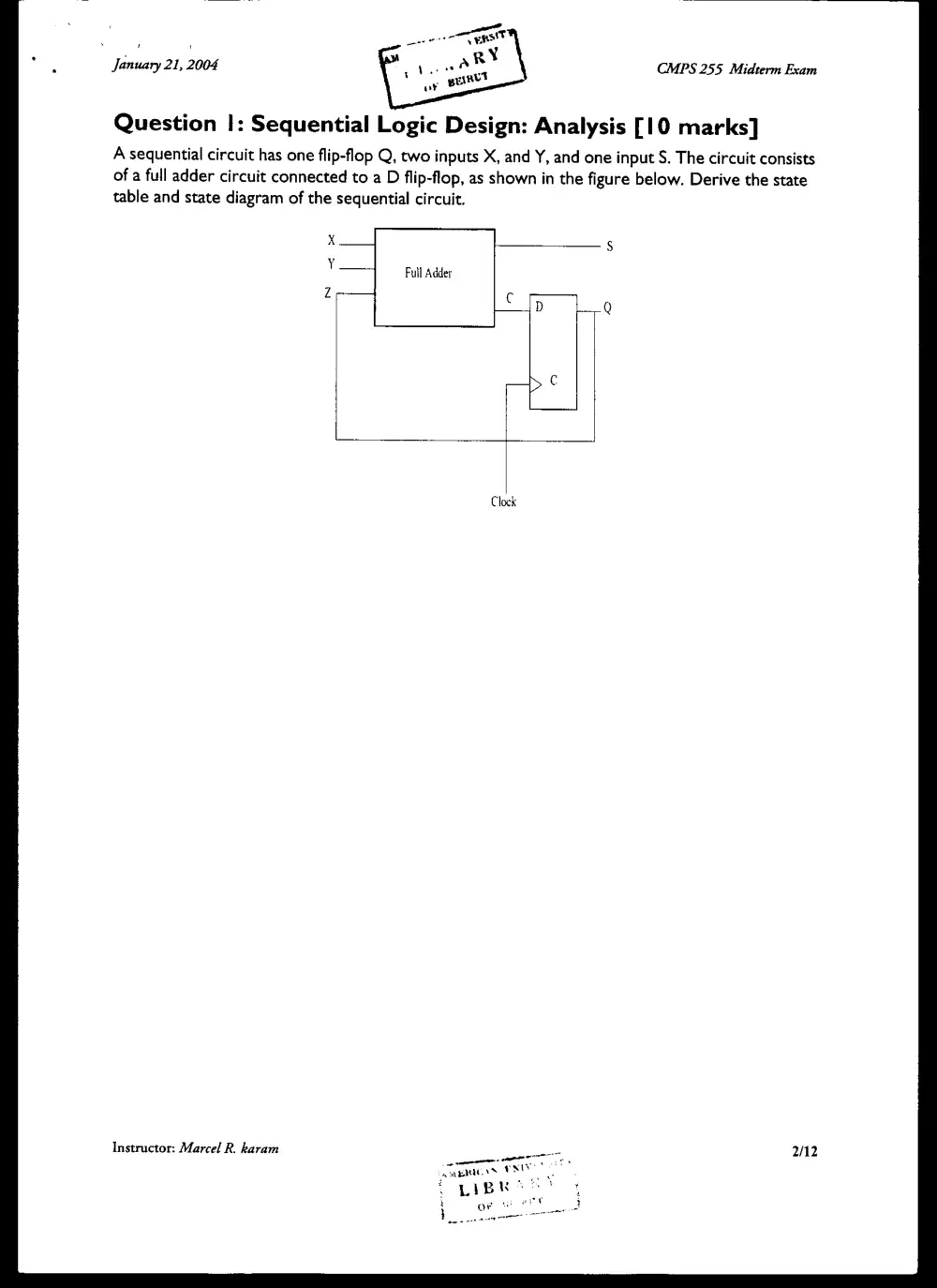
Question |: Sequential Logic Design: Analysis [10 marks]
A sequential circuit has one flip-flop Q, two inputs X, and Y, and one input S. The circuit consists
of a full adder circuit connected to a D flip-flop, as shown in the figure below. Derive the state
table and state diagram of the sequential circuit.
x__| JS
V—J pull Adder
Z
Cc D Q
c
Clock
Instructor: Marcel R. karam a 2/12
nn NO
Saiaeas UNIWERST
LIBRARY
oF BEIRUT
January 21, 2004
CMPS 255 Midterm Exam
Question 2: Sequential Logic Design: Implementation [ts
marks]
Design a sequential circuit with two JK flip-flops A and B and one input X. When X = 0, the state
of the circuit remains the same. When X = I, the circuit goes through the state transition from
00 to 10 to II to 01, back to 00, and repeats.
Instructor: Marcel R. karam 3/12
MEHICAN ENIVERSIT
LIBRARY
OF BEIRDT
January 21, 2004
CMPS 255 Midterm Exam
Question 3 State Machine Design [10 marks]
Create a state transition diagram for a machine that computes an even parity bit z for its ewo-bit
input xx. The machine outputs a 0 when all of the previous two-bit inputs collectively have an
even number of I's, and outputs a 1 otherwise. For the initial state, assume that the machine
starts with even parity.
Question 4: Memory Design [10 points]
A) How many 32 X 8 RAM chips are needed to provide a memory capacity of | MB
B) A program compiled for a SPARC ISA writes the 32-bit unsigned integer OxABCDEFO! to a
file and reads it back correctly. The same program compiled for a Pentium ISA also works cor-
rectly. However, when the file is transferred between machines, the program incorrectly reads
the integer from the file as OxEFCDAB. What is going wrong?
Instructor: Marcel R. karam
eee
MERICaS UNI VERS
January 21, 2004 LIBRARY CMPS 255 Midterm Exam
oF LFIROT
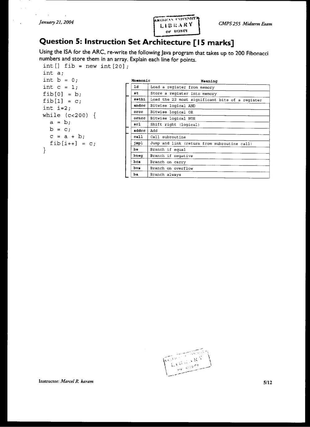
Question 5: Instruction Set Architecture [15 marks]
Using the ISA for the ARC, re-write the following Java program that takes up to 200 Fibonacci
numbers and store them in an array. Explain each line for points.
int[] fib = new int [20];
int a;
int b Mnemonic Meaning
int c ld Load a register from memory
fib {o] at Store a register into memory
. Load the 22 most significant bits of a register
fib[1] g 2
Bitwise logical AND
int i= Bitwise logical OR
Bitwise logical NOR
Shift right (logical)
Add
Call subroutine
Jump and link (return from subroutine call}
Branch if equal
Branch if negative
Branch on carry
Branch on overflow
Branch always
Instructor: Marcel R. karam
' t tml enna aneneeatenatall
5 ERICAN CNIVERSIT
January 21, 2004 ID RARY CMPS 255 Midterm Exam
OF BRIRTE
Question 6 Counters [15 marks]
Use JK-type flip-flops to design a counter with the following repeated binary sequence: 0, 1,2.
Instructor: Marcel R. karam
MERICAN CNIVERSIT '
LIBRARY
op RVIRDT
° 8 January 21, 2004 CMPS 255 Midterm Exam
Question 7 Boolean Algebra [5 marks]
Use the properties of Boolean Algebra to prove the Demorgan’s Theorem algebraically
Instructor: Marcel R. karam W2
eee
‘ Premaee {vunsiT
: % EAN EN .
January 21, 2004 LIBRARY
OF BEANTT
CMPS 255 Midterm Exam
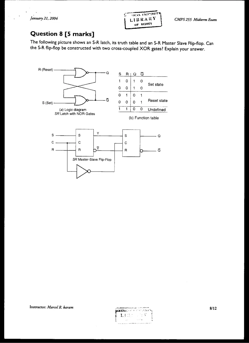
Question 8 [5 marks]
The following picture shows an S-R latch, its truth table and an S-R Master Slave Flip-flop. Can
the S-R flip-flop be constructed with two cross-coupled XOR gates? Explain your answer.
R (Reset) _
Q S RQ Gd
1 Oj; 1 +0
Set state
Oo O}/1 0
0 1/0 1
Q Reset state
S (Set} 0 0/0 1 —
(a) Logic diagram 1 1/{0 O Undefined
SR Latch with NOR Gates
(b) Function table
Ss $s Y SS) Q
C +4 ¢ c
R R bY R om a
SR Master-Slave Flip-Flop
>
Instructor: Marcel R. karam 8/12
January 21, 2004 po COMPS. 255 Midterm Exam
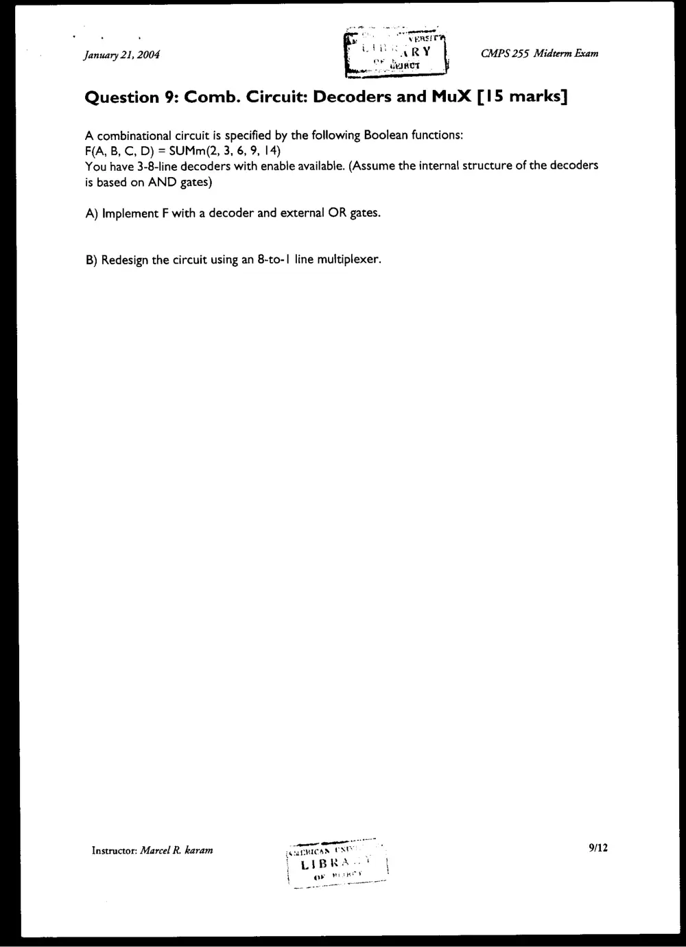
Question 9: Comb. Circuit: Decoders and MuX [15 marks]
A combinational circuit is specified by the following Boolean functions:
F(A, B, C, D) = SUMm(2, 3, 6, 9, 14)
You have 3-8-line decoders with enable available. (Assume the internal structure of the decoders
is based on AND gates)
A) Implement F with a decoder and external OR gates.
B) Redesign the circuit using an 8-to-| line multiplexer.
eee emma
Instructor: Marcel R. karam HMERICAN EXT
PT LEBRA ft
{ aw rene
,
January 21, 2004 ERIGAS CNIVERSIT CMPS 255 Midterm Exam
LIBRARY
OP BEIRTT
Instructor: Marcel R. karam