
CMPS 255 Final, Fall 2003
American University of Beirut · Computer Architecture · 6 pages



More CMPS 255 files
Show the text of this final exam
American University of Beirut
Faculty of Arts and Science,
Department of Computer Science
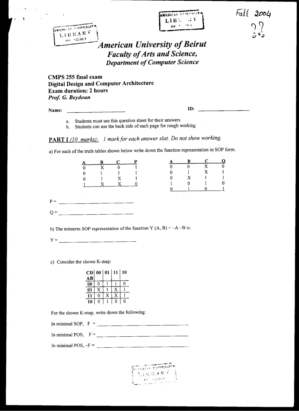
CMPS 255 final exam
Digital Design and Computer Architecture
Exam duration: 2 hours
Prof. G. Beydoun
Name: ID:
a. Students must use this question sheet for their answers
b. Students can use the back side of each page for rough working
PARTI (10_marks): 1 mark for each answer slot. Do not show working.
a) For each of the truth tables shown below write down the function representation in SOP form.
Q
0
1
1
0
1
P=
Q=
b) The minterm SOP representation of the function Y (A, B) = ~A -Bis:
Y=
c) Consider the shown K-map:
CD] 00 | 01] i1
AB
00 1]
01 1|X
ll XX
10 1|0
For the shown K-map, write down the following:
In minimal SOP, F =
In minimal POS, F
In minimal POS, ~F =
d) Write down the expression of the function f(A, B, C, D) implemented by the shown circuit. Note A and
B are contro! inputs (i.e. select lines).
B>
~C+D7>
cS
D>
4to]
Multiplexer > f(A, B,C, D)
R and § are implemented by the following circuits. Note B is the control input (i.e. the select line):
A> [hb
~AD] I 2t01
~BD{1S Multiplexer
~A>
A>
B> |S Multiplexer
F(R, S)=RS+-~R~S
Write down F in terms of A and B:
F(A, B)=
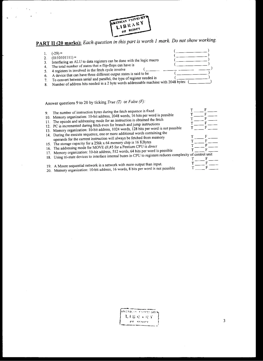
PART II (20 marks): Each question in this part is worth 1 mark. Do not show working.
1, (-29)= ( )
2. (QLIO101111)= ( )
3. Interfacing an ALU to data registers can be done with the logic macro ( }
4, The total number of states that » flip-flops can have is ( )
5, 4 registers in involved in the fetch cycle involve ( )
6. Adevice that can have three different output states is said to be ( )
7. Toconvert between serial and parailel, the type of register needed is ( »)
8. Number of address bits needed in a 2 byte words addressable machine with 2048 bytes: )
Answer questions 9 to 20 by ticking True (T) or False (F):
9. The number of instruction bytes during the fetch sequence is fixed T
10. Memory organization: 10-bit address, 2048 words, 16 bits per word is possible T
11. The opcode and addressing mode for an instruction is obtained the fetch T
12. PC is incremented during fetch even for branch and jump instructions T
13. Memory organization: 10-bit address, 1024 words, 128 bits per word is not possible T
14. During the execute sequence, one or more additional words containing the
operands for the current instruction will always be fetched from memory T
15. The storage capacity for a 256k x 64 memory chip is 16 KBytes T
16. The addressing mode for MOVE d1,#5 fora Pentium CPU is direct T
17. Memory organization: 10-bit address, 512 words, 64 bits per word is possible T
18. Using tri-state devices to interface internal buses in CPU to registers reduces complexity of control unit
T
19, A Moore sequential network is a network with more output than input. T
20. Memory organization: 10-bit address, 16 words, 8 bits per word is not possible T
[Dan ene nes
BAMEMIC 8 ryey
Lipraky
OP nes 3
3
Part III (13 marks):
A sequential circuit has one input X and one output Z. If the input X is 1, the circuit counts in the sequence:
011, 001, 110, 010, 111, 100, 101, 011,... Ifthe input X is 0, the circuit counts in the sequence: 011, 110,
001, 111,010, 101, 100, 011, ... Each time the count is 100, the circuit outputs |.
a) Draw the state diagram of the behaviour of the circuit (4 marks)
b) Give the transition table of the circuit (2 marks)
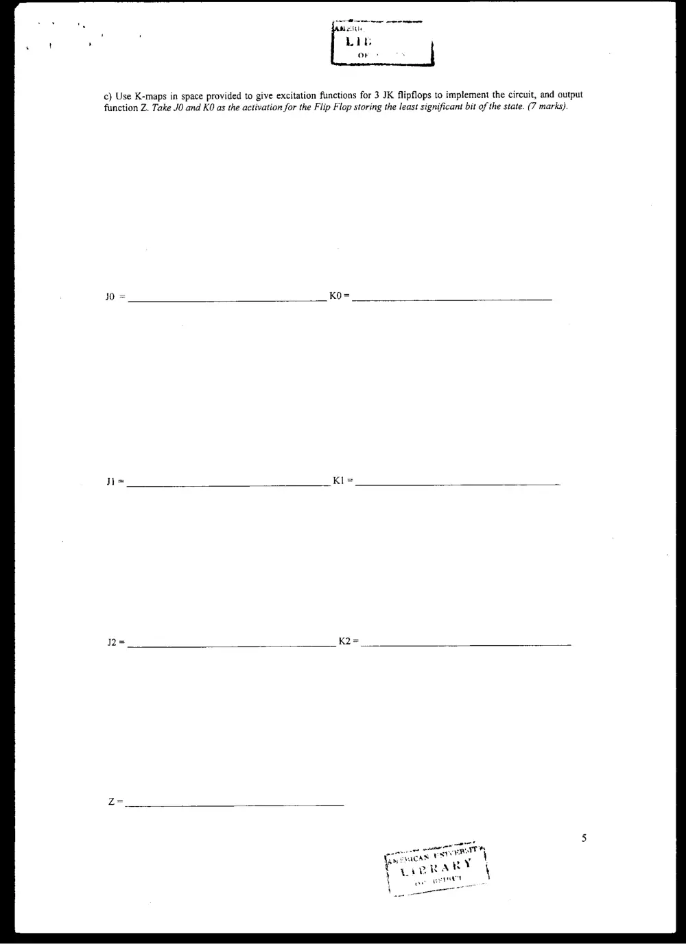
c) Use K-maps in space provided to give excitation functions for 3 JK flipflops to implement the circuit, and output
function Z. Take JO and KO as the activation for the Flip Flop storing the least significant bit of the state. (7 marks).
Part IV (8 marks):
b) (2 marks) The register transfer steps for bra #my_proc are:
d) (6 marks} Translate the following Java expression to assembly language. Use direct addressing mode
assuming that dO = a, dl = b, d2=c
inta=0,b=2,c=1;
while (c < (a+b) )
{
a=ct+b;
if(a<5)b ++;
ctt+;
= anne meneame
fstiacis VSIVERSIT
fvipeanwy
! Bizak y
if PCLIRUG