
CMPS 255 Final, Fall 2005
American University of Beirut · Computer Architecture · 8 pages

More CMPS 255 files
Show the text of this final exam
American University of Beirut
Faculty of Arts and Science,
Department of Computer Science
CMPS 255 final exam
Computer Architecture
Exam duration: 2 hours
Name: ________________________
ID: _____________________
a.
Students must use this question sheet for their answers
b.
Students must use ink, however they may use pencil and ruler for drawings.
c.
Students have 10 minutes reading time
d.
Students can use the back side of each page for rough working
PART I (20 marks): Do not show working, each question is 4 marks.
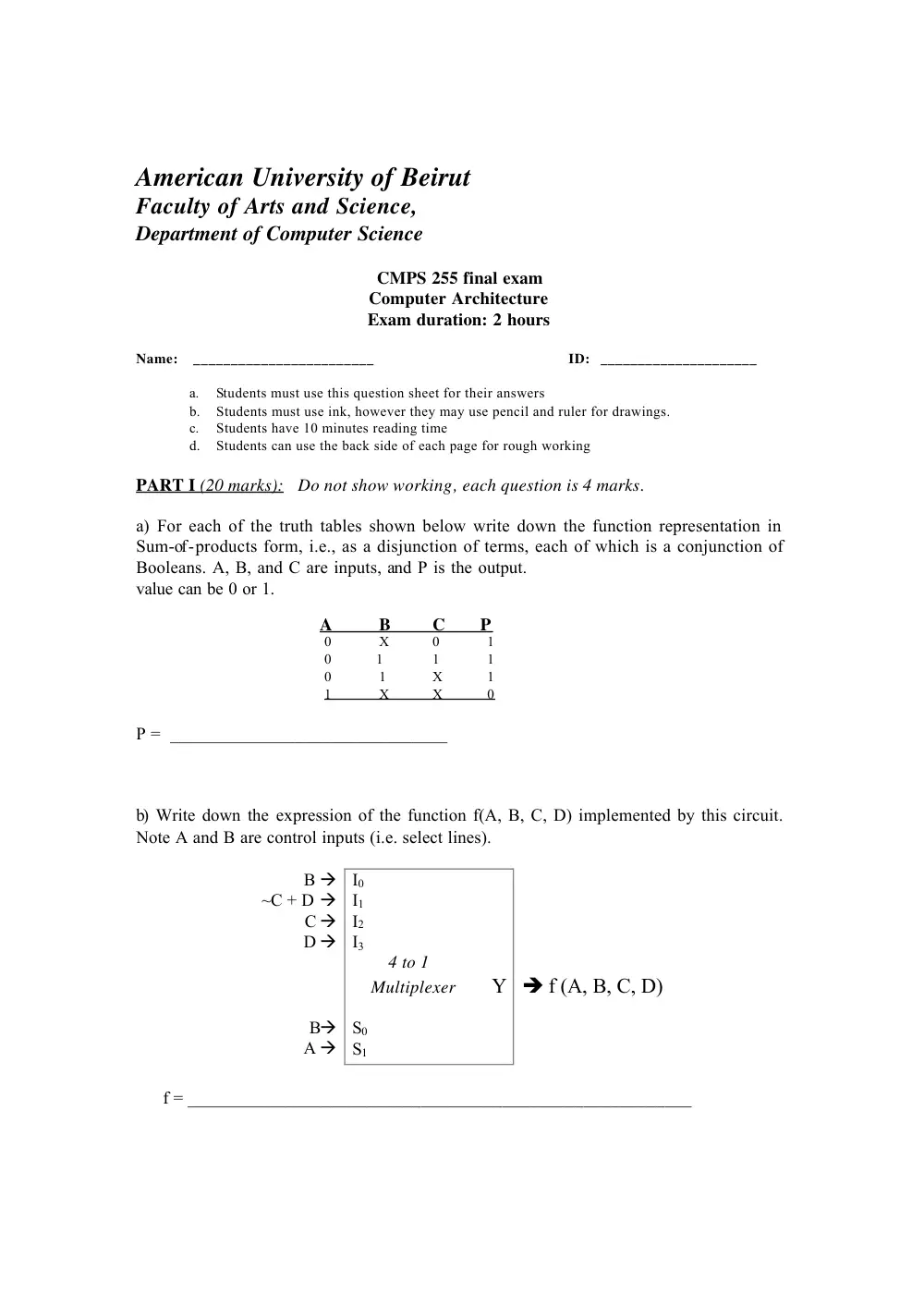
a) For each of the truth tables shown below write down the function representation in
Sum-of-products form, i.e., as a disjunction of terms, each of which is a conjunction of
Booleans. A, B, and C are inputs, and P is the output.
value can be 0 or 1.
A
B C P
0
X
0
1
0 1
1
1
0
1
X
1
1
X
X
0
P = _______________________________
b) Write down the expression of the function f(A, B, C, D) implemented by this circuit.
Note A and B are control inputs (i.e. select lines).
B �
~C + D �
C �
D �
B�
A �
I0
I1
I2
I3
4 to 1
Multiplexer Y
S0
S1
� f (A, B, C, D)
f = ________________________________________________________
2
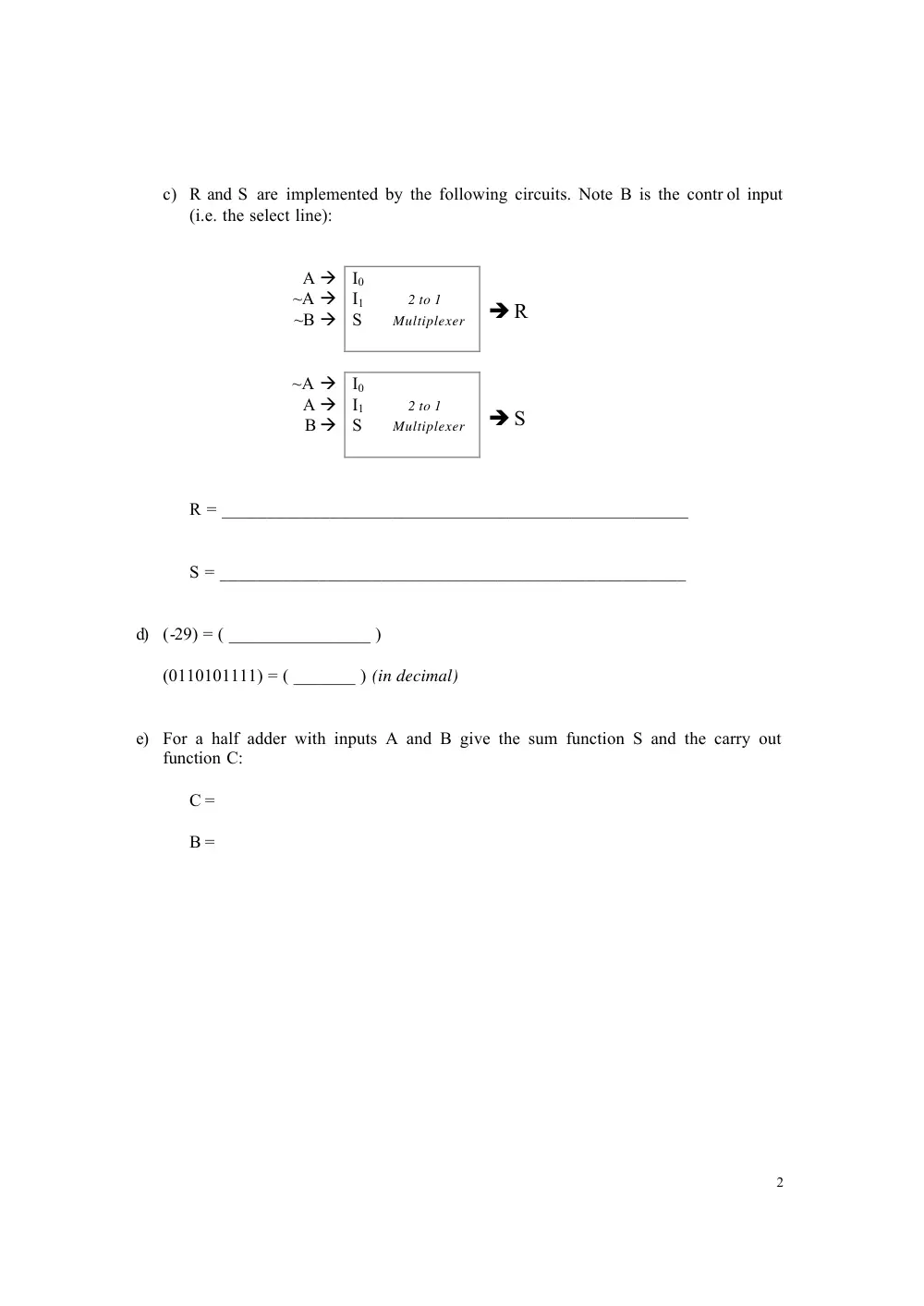
c) R and S are implemented by the following circuits. Note B is the contr ol input
(i.e. the select line):
A �
~A �
~B �
I0
I1 2 to 1
S Multiplexer
� R
~A �
A �
B �
I0
I1 2 to 1
S Multiplexer
� S
R = ____________________________________________________
S = ____________________________________________________
d) (-29) = ( ________________ )
(0110101111) = ( _______ ) (in decimal)
e) For a half adder with inputs A and B give the sum function S and the carry out
function C:
C =
B =
3
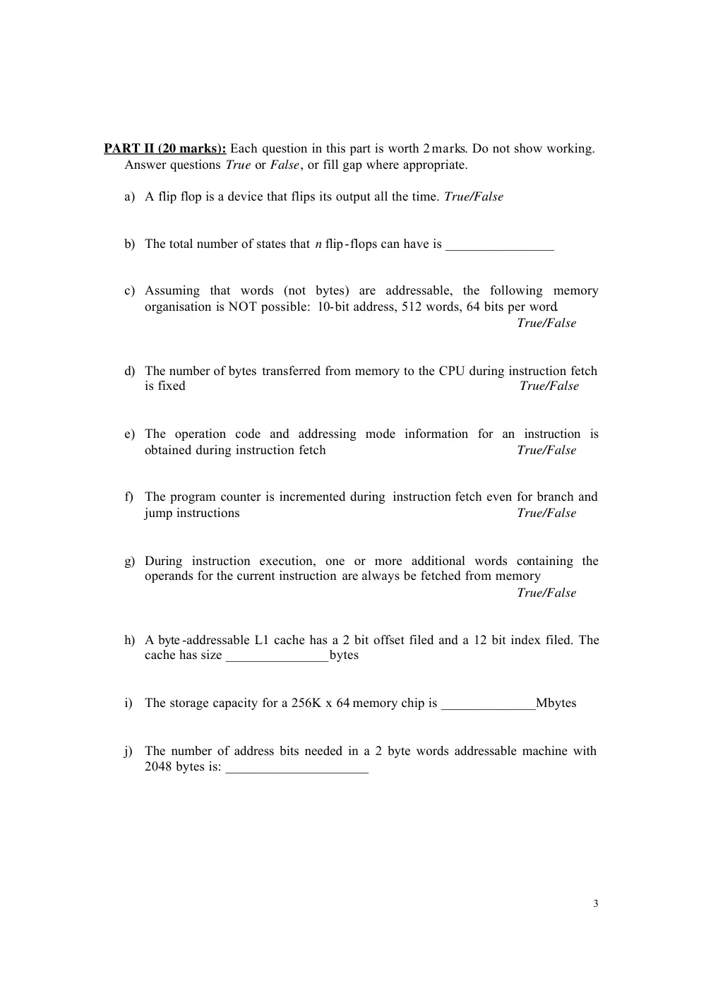
PART II (20 marks): Each question in this part is worth 2 marks. Do not show working.
Answer questions True or False, or fill gap where appropriate.
a) A flip flop is a device that flips its output all the time. True/False
b) The total number of states that n flip-flops can have is ________________
c) Assuming that words (not bytes) are addressable, the following memory
organisation is NOT possible: 10-bit address, 512 words, 64 bits per word.
True/False
d) The number of bytes transferred from memory to the CPU during instruction fetch
is fixed
True/False
e) The operation code and addressing mode information for an instruction is
obtained during instruction fetch
True/False
f) The program counter is incremented during instruction fetch even for branch and
jump instructions
True/False
g) During instruction execution, one or more additional words containing the
operands for the current instruction are always be fetched from memory
True/False
h) A byte -addressable L1 cache has a 2 bit offset filed and a 12 bit index filed. The
cache has size _______________bytes
i) The storage capacity for a 256K x 64 memory chip is ______________Mbytes
j) The number of address bits needed in a 2 byte words addressable machine with
2048 bytes is: _____________________
4
Part III (30 marks):
For this part you have two options (equally marked), do only ONE.
OPTION A:
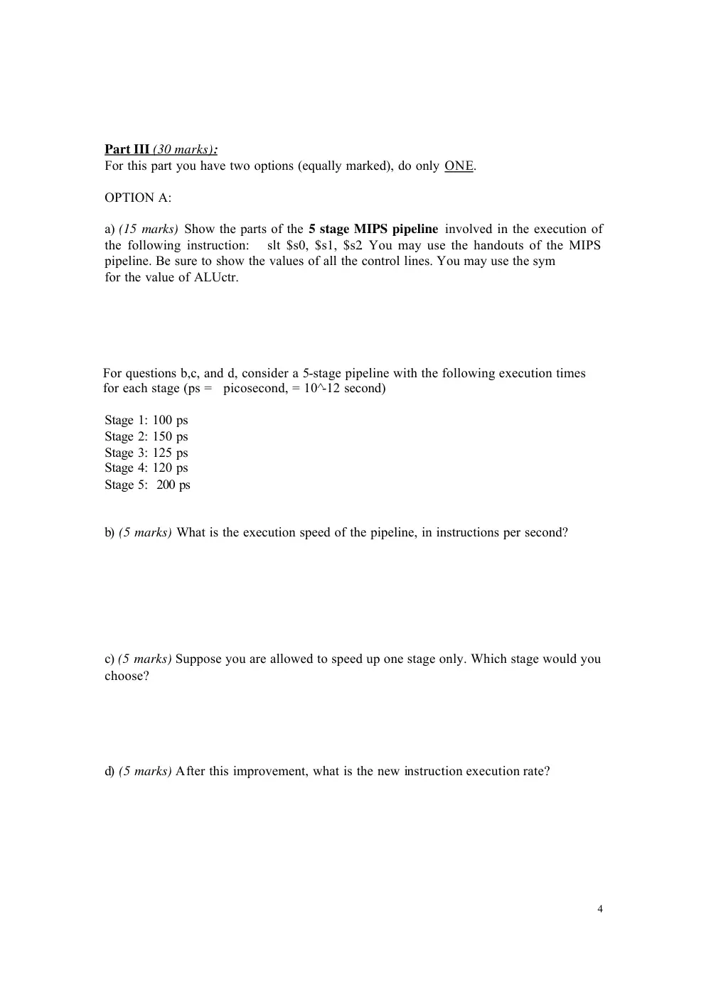
a) (15 marks) Show the parts of the 5 stage MIPS pipeline involved in the execution of
the following instruction: slt $s0, $s1, $s2. You may use the handouts of the MIPS
pipeline. Be sure to show the values of all the control lines. You may use the sym
for the value of ALUctr.
For questions b,c, and d, consider a 5-stage pipeline with the following execution times
for each stage (ps = picosecond, = 10^-12 second)
Stage 1: 100 ps
Stage 2: 150 ps
Stage 3: 125 ps
Stage 4: 120 ps
Stage 5: 200 ps
b) (5 marks) What is the execution speed of the pipeline, in instructions per second?
c) (5 marks) Suppose you are allowed to speed up one stage only. Which stage would you
choose?
d) (5 marks) After this improvement, what is the new instruction execution rate?
5
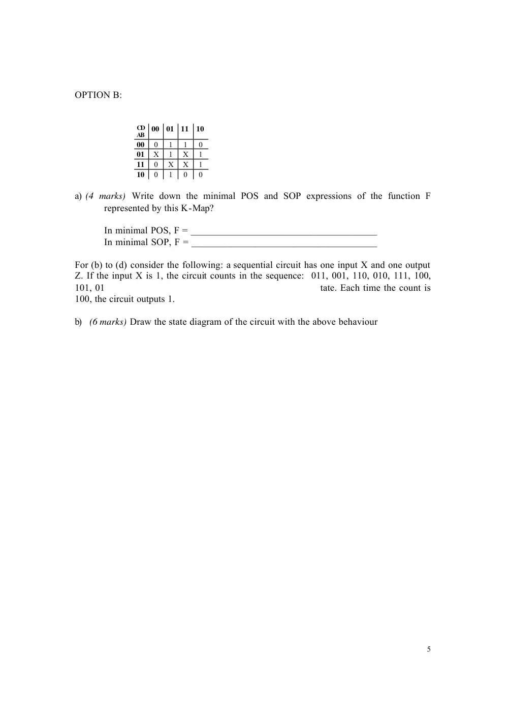
OPTION B:
CD
AB 00 01 11 10
00
0
1
1
0
01 X
1
X
1
11
0
X
X
1
10
0
1
0
0
a) (4 marks) Write down the minimal POS and SOP expressions of the function F
represented by this K-Map?
In minimal POS, F = ______________________________________
In minimal SOP, F = ______________________________________
For (b) to (d) consider the following: a sequential circuit has one input X and one output
Z. If the input X is 1, the circuit counts in the sequence: 011, 001, 110, 010, 111, 100,
101, 01
tate. Each time the count is
100, the circuit outputs 1.
b) (6 marks) Draw the state diagram of the circuit with the above behaviour
6
c) (8 marks) Give the transition table
d) (12 marks )Give minimized (in SOP form) excitation functions for 3 JK flip flops
to produce the above transition table, and the Boolean function Z for the output
J0 = ________________________________________
K0 = ________________________________________
J1 = _________________________________________
K1 = _________________________________________
J2 = __________________________________________
K2 = __________________________________________
Z = ____________________________________________
7
Part IV (30 marks)
a) (10 marks)
For MIPS datapath, show the parts of the single-cycle involved in the execution of the
following instruction: slt $s0, $s1, $s2. You may use the handout of the MIPS single
cycle datapath. Be sure to show the values of all the control lines. You may use the
OR
For M68K answer following:
(2 mark)
The addressing mode for MOVE #5, d0 is ___________________
(4 marks)
Name the 4 registers in the M68K CPU are involved in the fetch cycle:
__________________________
(4 marks)
Show the register transfer steps for bra #my_proc:
b) (12 marks) Translate the following Java expression to assembly language. Use direct
addressing mode assuming that registers d0, d1 and d2 store a, b and c respectively.
int a, b = 1, c = 2;
while ( c < 8)
{
a = c + b;
if ( a < 5) b ++;
c ++;
}
8
c) (8 marks) You are given a system with a level 1 cache and a main memory, with the
following specification:
Cache cycle time: 1ns
Cahce hit rate: 99%
Main memory cycle time: 100ns
Compute the average memory access time