
EECE 312L Notes Experiment 10 Notes, Fall 2013
American University of Beirut · Circuits and Electronics Lab · 4 pages

More EECE 312L files
- Notes Experiment 3 Notes · Fall 2013NotesView
- Notes Experiment 4 Notes · Fall 2013NotesView
- Notes Experiment 2 Notes · Fall 2013NotesView
- Notes Experiment 7 Noes · Fall 2013NotesView
- Notes Experiment 5 Notes · Fall 2013NotesView
- Notes Experiment 6 Notes · Fall 2013NotesView
- Notes Experiment 11 Notes · Fall 2013NotesView
- Notes Experiment 1 Notes · Fall 2013NotesView
Show the text of this notes
Experiment 10
MOS Transistor
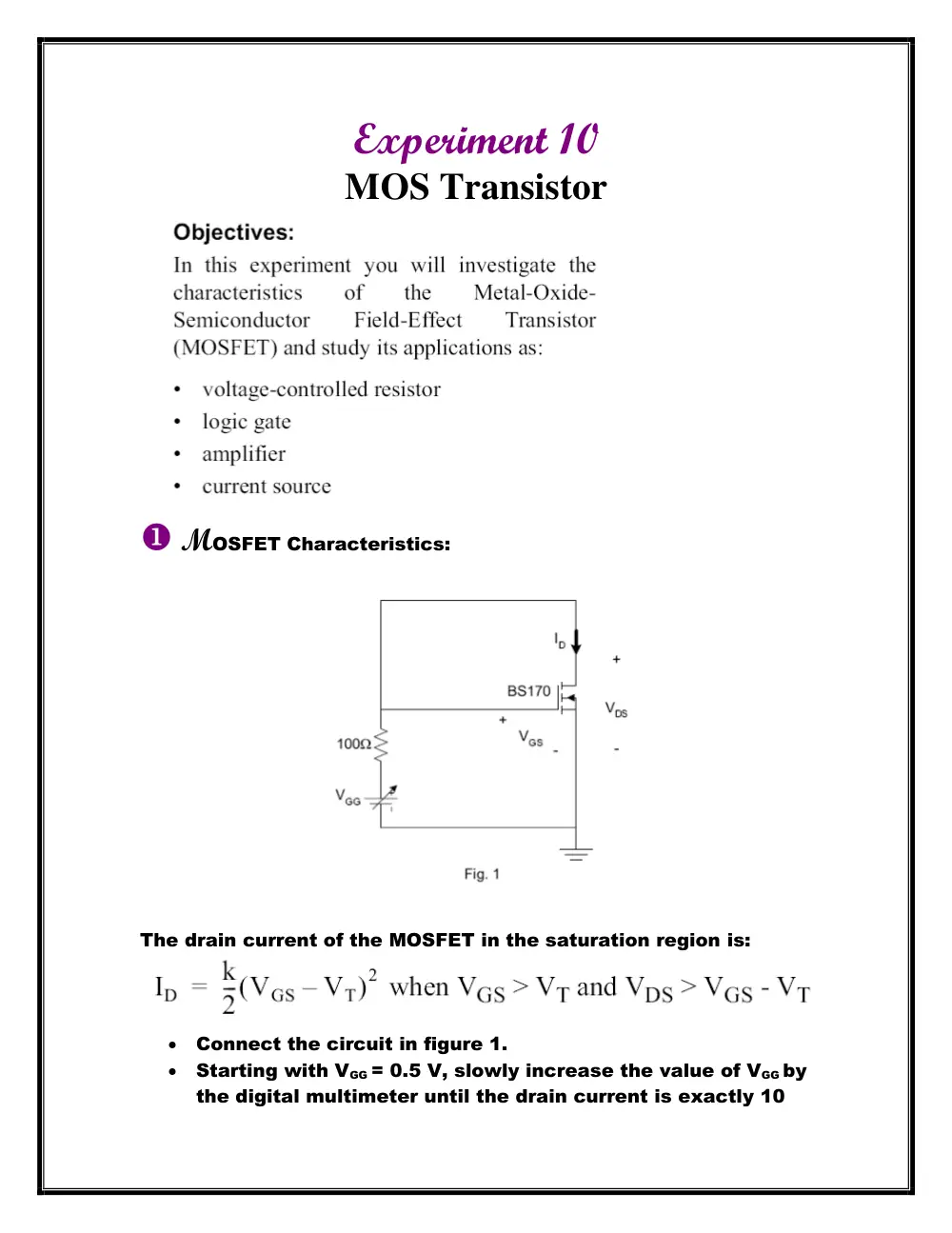
MOSFET Characteristics:
The drain current of the MOSFET in the saturation region is:
Connect the circuit in figure 1.
Starting with VGG = 0.5 V, slowly increase the value of VGG by
the digital multimeter until the drain current is exactly 10
mA. Read the value of VGS. Increase VGG further until the
drain current is exactly 25 mA. Read the value of VGS.
Now we have two different values of IS and VGS and thus we
could now solve two equations with two unknowns to find
the trans conductance parameter k and the threshold
voltage VT according to the above equation.
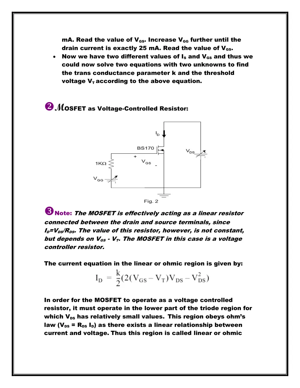
MOSFET as Voltage-Controlled Resistor:
Note: The MOSFET is effectively acting as a linear resistor
connected between the drain and source terminals, since
ID=VDS/RDS. The value of this resistor, however, is not constant,
but depends on VGS - VT. The MOSFET in this case is a voltage
controller resistor.
The current equation in the linear or ohmic region is given by:
In order for the MOSFET to operate as a voltage controlled
resistor, it must operate in the lower part of the triode region for
which VDS has relatively small values. This region obeys ohm’s
law (VDS = RDS ID) as there exists a linear relationship between
current and voltage. Thus this region is called linear or ohmic
because the MOSFET is working as a resistor controlled by a
voltage.
MOSFET Logic Gate:
NOR GATE
We see that the logic function is true only for IN1 and IN2 are both
false; it is false otherwise. This circuit thus implements the NOR
logic function that is we get VOUT = (VIN1 OR VIN 2)’.
This circuit implements a logic gate; there are two inputs IN1 and
IN2, and one output OUT.
To build the truth table of this gate, we apply all possible
combinations of inputs, and observe the output. Start with IN1 =
logic 0 and IN2 = logic 0. To get a logic 0, we will connect the
input nodes to ground. What is the value of the output in this
case? This is the value of voltage that corresponds to logic 1.
Apply logic 1 at IN1, and logic 0 at IN2, and observe the output.
Note The MOSFET must be in the saturation region to use it as an
amplifier.
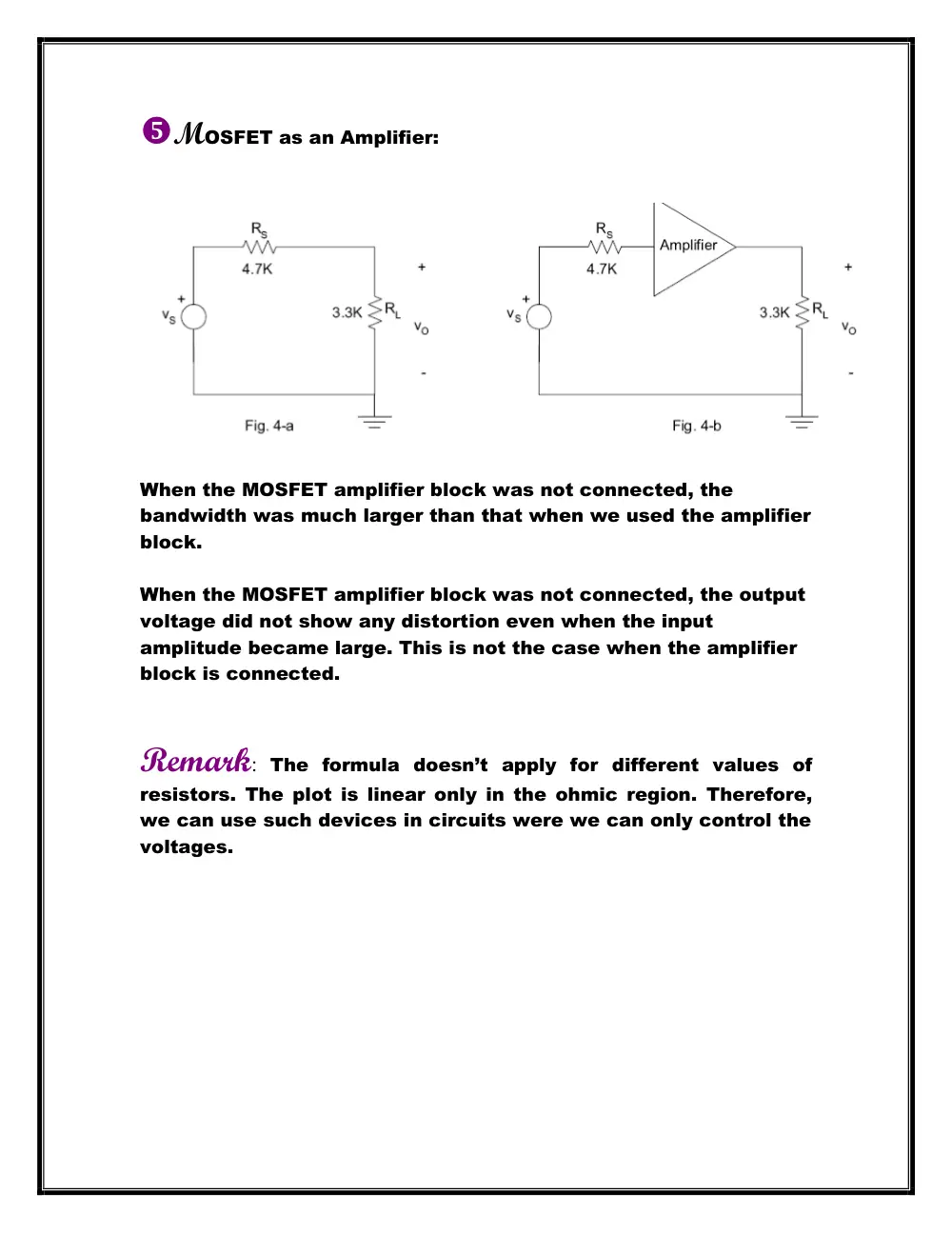
MOSFET as an Amplifier:
When the MOSFET amplifier block was not connected, the
bandwidth was much larger than that when we used the amplifier
block.
When the MOSFET amplifier block was not connected, the output
voltage did not show any distortion even when the input
amplitude became large. This is not the case when the amplifier
block is connected.
Remark: The formula doesn’t apply for different values of
resistors. The plot is linear only in the ohmic region. Therefore,
we can use such devices in circuits were we can only control the
voltages.