
EECE 312L Notes Experiment 11 Notes, Fall 2013
American University of Beirut · Circuits and Electronics Lab · 6 pages



More EECE 312L files
- Notes Experiment 3 Notes · Fall 2013NotesView
- Notes Experiment 4 Notes · Fall 2013NotesView
- Notes Experiment 2 Notes · Fall 2013NotesView
- Notes Experiment 7 Noes · Fall 2013NotesView
- Notes Experiment 5 Notes · Fall 2013NotesView
- Notes Experiment 6 Notes · Fall 2013NotesView
- Notes Experiment 10 Notes · Fall 2013NotesView
- Notes Experiment 1 Notes · Fall 2013NotesView
Show the text of this notes
Experiment 11
Bipolar Junction Transistor
BJT Characteristics:
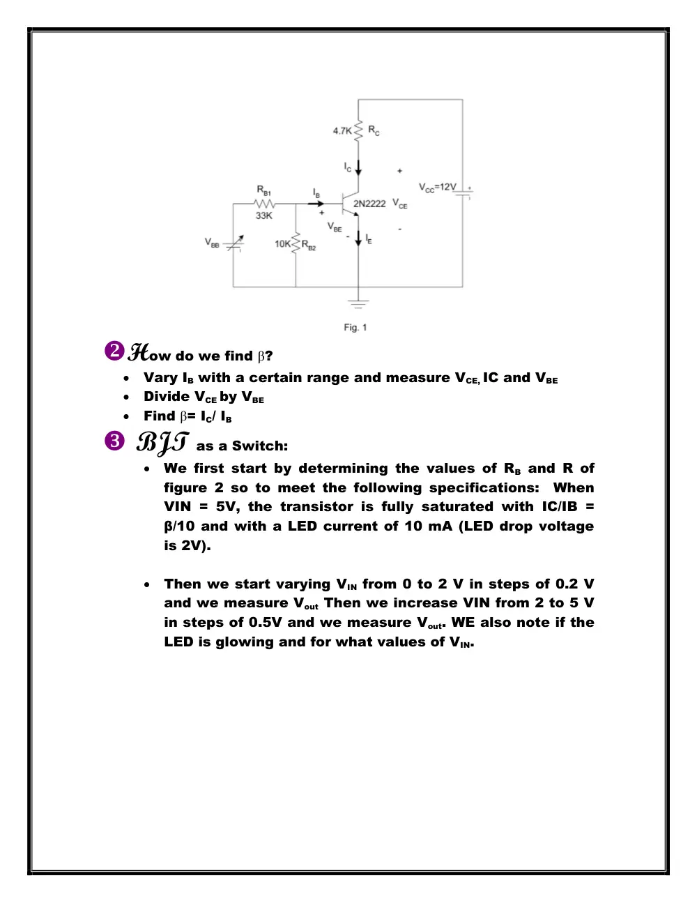
We first start by connecting the circuit of figure 1 which
will be used to determine the characteristics of the
2N222 BJT, and its different regions of operations.
We start with VBB = 1 V, and we increase VBB to 8 V in
steps of 0.2V. While measuring the collector current IC,
the Base current IB, the collector-to- emitter voltage
VCE, and the base-to-emitter-voltage VBE.
In the active or the saturation region:
0.7< VBE <0.8
In the saturation region: VCE= 0.2 V
In the saturation region: VCE> 0.2 V
How do we find β?
Vary IB with a certain range and measure VCE, IC and VBE
Divide VCE by VBE
Find β= IC/ IB
BJT as a Switch:
We first start by determining the values of RB and R of
figure 2 so to meet the following specifications: When
VIN = 5V, the transistor is fully saturated with IC/IB =
β/10 and with a LED current of 10 mA (LED drop voltage
is 2V).
Then we start varying VIN from 0 to 2 V in steps of 0.2 V
and we measure Vout Then we increase VIN from 2 to 5 V
in steps of 0.5V and we measure Vout. WE also note if the
LED is glowing and for what values of VIN.
Switch:
ON → SATURATION
OFF→ CUTOFF
The drop across the BJT is very small. if it increases then
there would be too much heat and thus the transistor would
burn out.
The drop across the transistor could be calculated using the
formula: (VCC- o.2). If we divide this value by the current I we
calculate the resistor’s value Rc.
General Remarks:
A transistor is a current controlled device.
In a transistor the base current defines which region we
would be working in.
A MOSFET is a voltage controlled device.
We usually take a constant value of β throughout the
experiment.
How do we measure IB?
At the edge of saturation or in the active region only IC= β IB
If we use a value of β equal to 100 we might burn the transistor.
Thus we have to increase β by a factor of 10 for example
(usually) and thus we would have β ‘ = β /10
The β force is the factor that forces the transistor to go to
saturation by β ‘ = β /10. Thus the current IB would increase and IC
would remain fixed with IC= (β /10) IB the RB could be calculated
by RB= (VCC - 0.7)/ IB calculated.
Connect the circuit in figure 2. Vary VIN from 0 V to 2 V in
steps of 0.2 V and measure VOUT (by the oscilloscope). Increase
VIN from 2 V to 5 V in steps of 0.5 V and measure VOUT. We also
note the value of VIN at which the LED starts glowing.
BJT as an Amplifier:
Why is the DC analysis important?
Point of operation Q (we need to get Q)
Place in small signal model and analyze
DC measurements: gm is needed to place the transistor in the
active region that is to check if the transistor is in the active
region.
VCE>0.3 VCC = 1/3 VCC
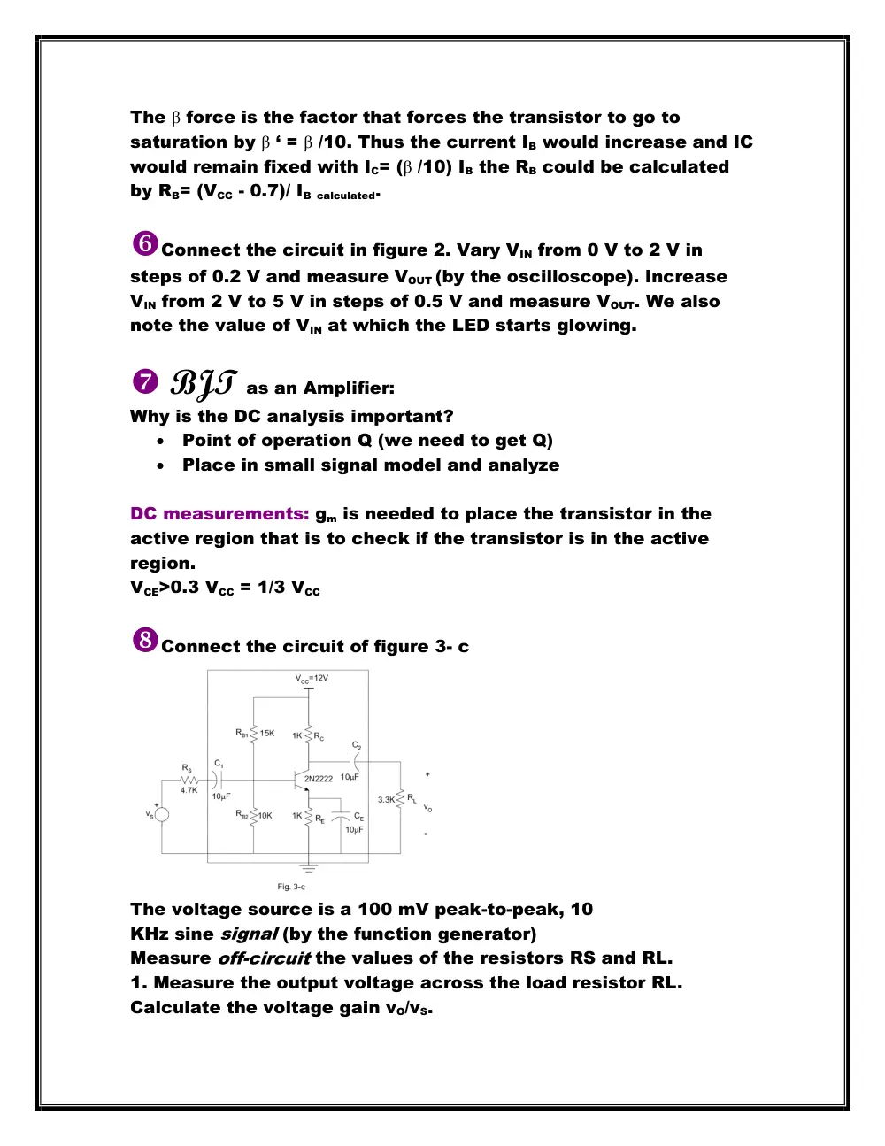
Connect the circuit of figure 3- c
The voltage source is a 100 mV peak-to-peak, 10
KHz sine signal (by the function generator)
Measure off-circuit the values of the resistors RS and RL.
1. Measure the output voltage across the load resistor RL.
Calculate the voltage gain vO/vS.
Note: Even thought the ratio vO/vS is less than 1, we still refer to
it as gain. When we connect the BJT amplifier block, the ratio
will become much larger than 1.
Vo is (Vs – Vi)/VCC - 0.3
And Vi = Vo/RL
Find Av= Vo / Vi
As we can see in the first 2 steps the gain does not change
though Vin is much bigger in step 2 then in 1 . This is because
the gain does don’t depend here on the amplitude of Vin . In fact
we have that Vout = (RL / (Rs + RL)) Vin, so the ratio Vout / Vin is
equal to RL / (Rs + RL) which is a constant (here it is equal to
0.41). As we can also see for low frequencies the gain is
approximately equal to RL/(Rs + RL) and for very high frequencies
the gain is much more less then RL / (Rs + RL). This is due to
coupling capacitance in the circuit.
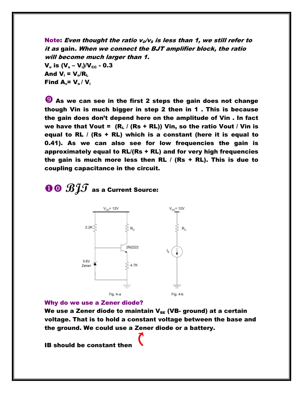
BJT as a Current Source:
Why do we use a Zener diode?
We use a Zener diode to maintain VBE (VB- ground) at a certain
voltage. That is to hold a constant voltage between the base and
the ground. We could use a Zener diode or a battery.
IB should be constant then
should be constant as well
Connect the circuit shown in Fig. 4-a. Start with RC = 0
(short circuit). We measure the base voltage and the emitter
voltage. Also measure off-circuit the value of the
4.7 KΩ emitter resistor.
Increase the value of RC from 0 to 12 KΩ using 1 KΩ, 1.5 KΩ, 2.2
KΩ, 2.7 KΩ, 3.3 KΩ, 4.7 KΩ, 5.6 KΩ, 6.8 KΩ, 8.2 KΩ, 10 KΩ, and 12
KΩ resistors, and measure the collector current of the transistor
and the collector-to-emitter voltage.
Note: RC should be measured off-circuit.
General Shape of the BJT