
EECE 320 Final, Fall 2005
American University of Beirut · Digital Systems Design · 8 pages




More EECE 320 files
- Final · Fall 2011Final examView
- Final · Fall 2010Final examView
- Final with Solutions · Fall 2009Final exam · with solutionView
- Problems For Final · Fall 2008Final examView
- Final with Solution · Fall 2005Final exam · with solutionView
- Homework 2 and 3 · Summer 2016HomeworkView
- Homework 1 · Summer 2016HomeworkView
- Homework 1 · Fall 2016HomeworkView
Show the text of this final exam
.
"'
"",..",
"',
,... -
. a-~.
.""". .&'-'.
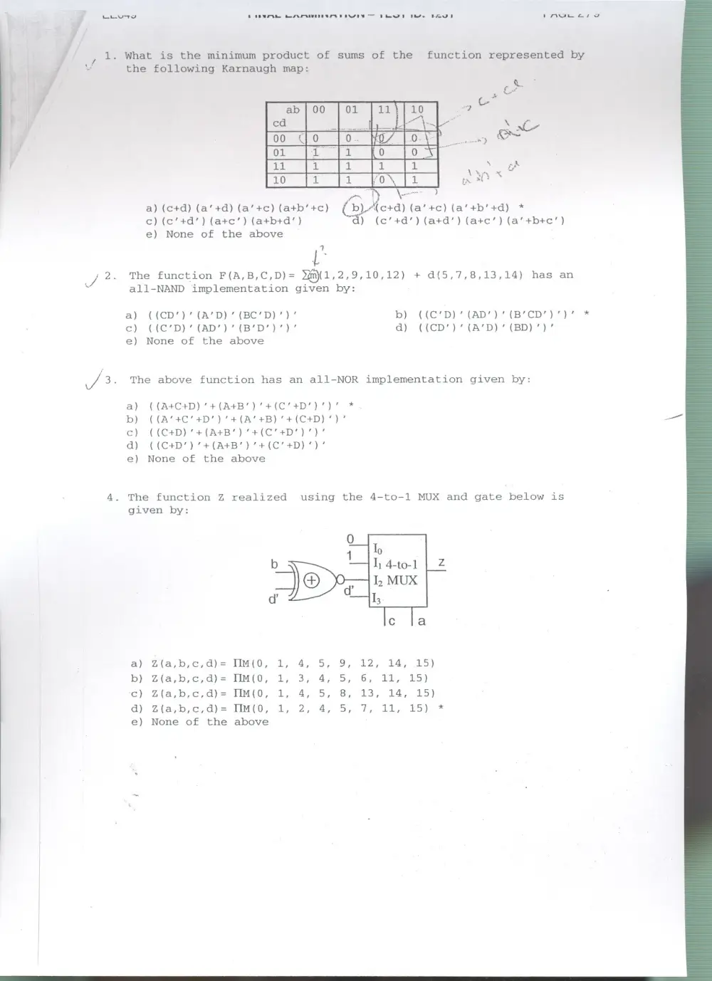
1. What
is the minimum
product
of sums
of
the
function
represented
by
f
',:
the following Karnaugh map:
ab
cd
00 (
01
11
10
01
00
10
,.,.'/\-
.
.-
0..
.![/
..0,
n1
0
0
111
' ~
" \
'
'or)
.'"
1
{0
1
(_,>-.
'I'
\
.
)
".-.
i J
I'b)/~c+d)
(a'+c)
(a'+b'+d)
*
'-d)
(c'+d')
(a+d')
(a+c')
(a'+b+c')
o
f....
1
1
a) (c+d) (a'+d)
(a'+c)
(a+b'+c)
c) (c'+d')
(a+c')
(a+b+d')
e)
None
of
the
above
.) 2.
(
The
funct.ion F(A,B,C,D)=
~(1,2,9,10,12)
+ d(5,7,8,13,14)
has
an
all-NAND
implementation
given
by:
a)
«CD')'
(A'D)' (BC'D)')'
c)
«C'D)'
(AD') ,(B'D')') ,
e) None
of
the
above
b)
«C'D)'
(AD') , (B'CD')
')'
*
d)
«
CD'
) , (A'
D)
, (BD)
, ) ,
vI'3.
The
above
function
has
an all-NOR
implementation
given
by:
a)
«A+C+D)'+(A+B')'+(C'+D')')'
*
b)
«A'+C'+D')'+(A'+B)'+(C+D)')'
c)
«C+D) '+(A+B')'+(C'+D')')'
d)
«C+D')'+(A+B')'+(C'+D)')'
e) None of the above
4. The function Z realized
using the 4-to-l MUX and gate below is
given by:
10
II4-to-lI Z
hMUX
13
C
la
a)
Z(a,b,c,d)=
ITM(O, 1, 4, 5,
9, 12,
14,
15)
b)
Z(a,b,c,d)=
ITM(O, 1, 3, 4, 5,
6, 11,
15)
'c)
Z (a, b, c , d) =
IIM
(0 ,
1, 4, 5, 8, 13,
14,
15)
d)
Z(a,b,c,d)=
IIM(O, 1, 2, 4, 5, 7,
11,
15)
*
e) None
of
the
above
.
",..,
"'"'.."'..
.__
v.
. r-.'-.A
L.
v
I
...,
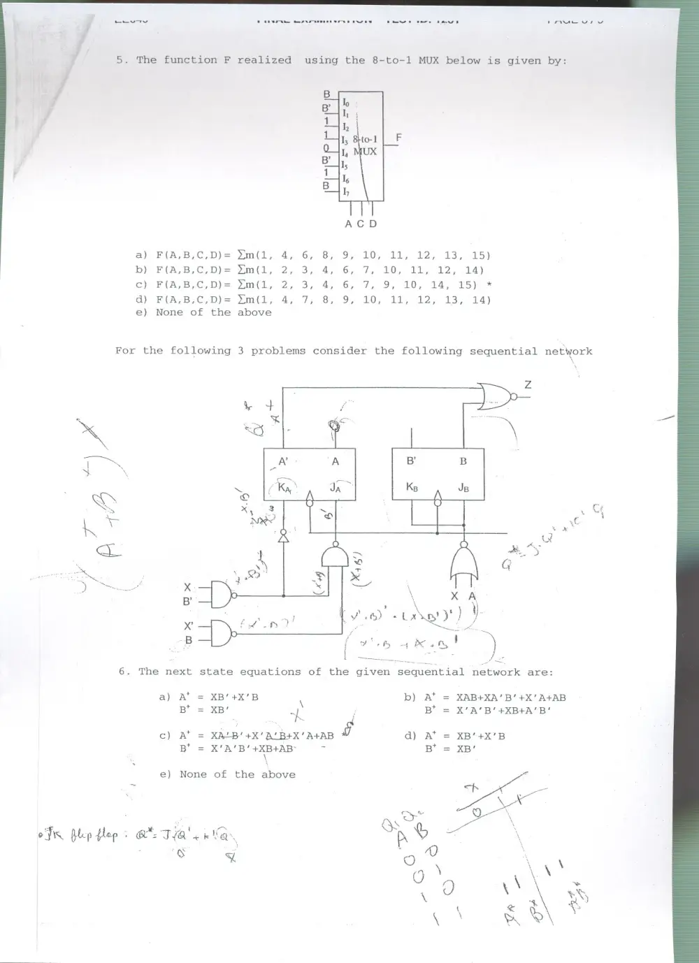
5. The
function
F realized
using
the
8-to-l
MUX
below
is given
by:
For
the
fol~owing
3 problems
consider
the
following
sequential
net,ork
~. ....
~
~ '\-
<:l:...
--~~
..)
'
/
A'
/"
X
B'
/~...
B'
B
KB
6.
The
next
state equations of the given sequential network are:
a)
A+
B+
XB'+X'B
XB'
\
1..
b)
A+ = XAB+XA'B'+X'A+AB
B+ = X'A'B'+XB+A'B'
,
c)
A+
B+
= XA-!-B'+X' ~+X'
A+AB
= X'A'B'+XB+AB-
\
e)
None of the above
d)
A+ = XB'+X'B
B+ = XB'
B
1
I,h
h Rl.tn-lI F
1=f
1
I,
B
16
17
ACD
a)
F(A,B,C,D)= Lm(l,
4,
6,
8,
9,
10,
11,
12,
13,
15 )
b)
F(A,B,C,D)= Lm(l,
2,
3,
4,
6,
7,
10,
11,
12,
14)
c)
F(A,B,C,D)=
Lm(l,
2,
3,
4,
6,
7,
9,
10,
14,
15)
*
d)
F(A,B,C,D)=
Lm(l,
4,
7,
8,
9,
10,
11,
12,
13,
14)
e)
None of the above
EE049
\
FINAL EXAMINATION
- TEST ID: 1231
PAGE4/9
7.
The
state
diagram of the given sequential network is:
1,0o
ffi
1,0o
ffi
(a)
(c)
(e)
None
of
the
above
1,0o@
1,0o
ffi
(b)
*
(d)
8. what are the first five output values, ignoring the initial output,
of the network for the input sequence x= 0 1 lOO?
a) 1 1 0 0 0
b) 0 0 1 1 0
c) 0 1 1 0 1
~
e) None of the above
~~~_~
The
following three problems tackle the design of a counter using 3
clocked
S-R
flip-flops,
named
ABC,
to
count
in
the
sequence:
000,
110,
111,
011,
000,
110
...
are
possible
input
values
of
flip-flop
A?
b)
SA= B'
& RA= A'
d)
SA= C'
& RA= A'C
}'.
10. Which
of
t
7
/ following
a}
SB= B'
R~
c}
SB= C'
RB= AC >
e} None
of
the above
are possible
input
values
of
flip-flop
B?
b}
SB= B'
& RB= A'
d}
SB= C' & RB= fP-c *
11. To
implement
the counter
the
three
flip-flops,
we
~'a
minimum configuration,
ne~
the following:
AND gate
in addition
to
a} Three
inverters
& one
b}
Three
inverters
only
c} One
AND
gate
only
*
d} Two
AND
gates
only
e} None
of
the above
The
following
two problems
tackle
the
design
of a counter
using
4
clocked
D flip-flops,
named
ABCD,
to count
in the
sequence:
o
3
6
o
3
9
12
15
12. Which
of
the
following
input values
of
flip-flops
ABC
lead
to
a ____
correct
design
with
min~
number
of gates?
'J
imPlem~ ~
\)
13. What
is
the minimum
the
counter?
of 2-input NAND
gates
needed
to
a} 8 *
e} None of the
d) 10
c) 7
The
following
three
problems
deal
with
the
design
of
a
sequence
detector.
The
detector
has
two
inputs
X
and
Y
and
one
output
z.
Initially z= 0 and XY= O~~
The
output
Z
is
set
to
1 when
you
apply
the
following input sequence
.
1~,
01,
otherwise
Z remains
O. Example:
\
\.
XY:
00
qo
11
00
tb 'I1>~~1'~ 10
11
01
01. ..
z:
0
~
0
0
0
0
1
0
0
1
0 ...
The
initial state Ts-'So- If you
apply an
input
state obtained is 81, And when in 81 you apply an
obtained is 82_..
In the following questions the
constructed
using
the
state
'names
80'
81,
82-__
sta~e
tab1e
should
be ordered
OO~
01~
10, and
11.
XY=10
when
in So, the
inputXY=11,
the- state
state
tables
should
be
The
inputs
XY
of
the
a}
D." BD'+=
BD'+A'D
Dc= BC' +A'B'
.--,
b}
DA= BD' +AB '.___.
DB= BC' +8' D
Dc= BC' +A' B'
*
r-- J 0
c}
DA=
BC'+A"
DB=
BC'+B'D
Dc=
C'D'+A'B'
I
l
'-....
d}
DA= AC'+'
DB= BC'+A'D
Dc= C'D'+A'B'
'"
e} None
of
the above
t::.t::.U4~
t"INAL t::.Jl.AMINA IIUN -
I t:::sI IU: 12;:11
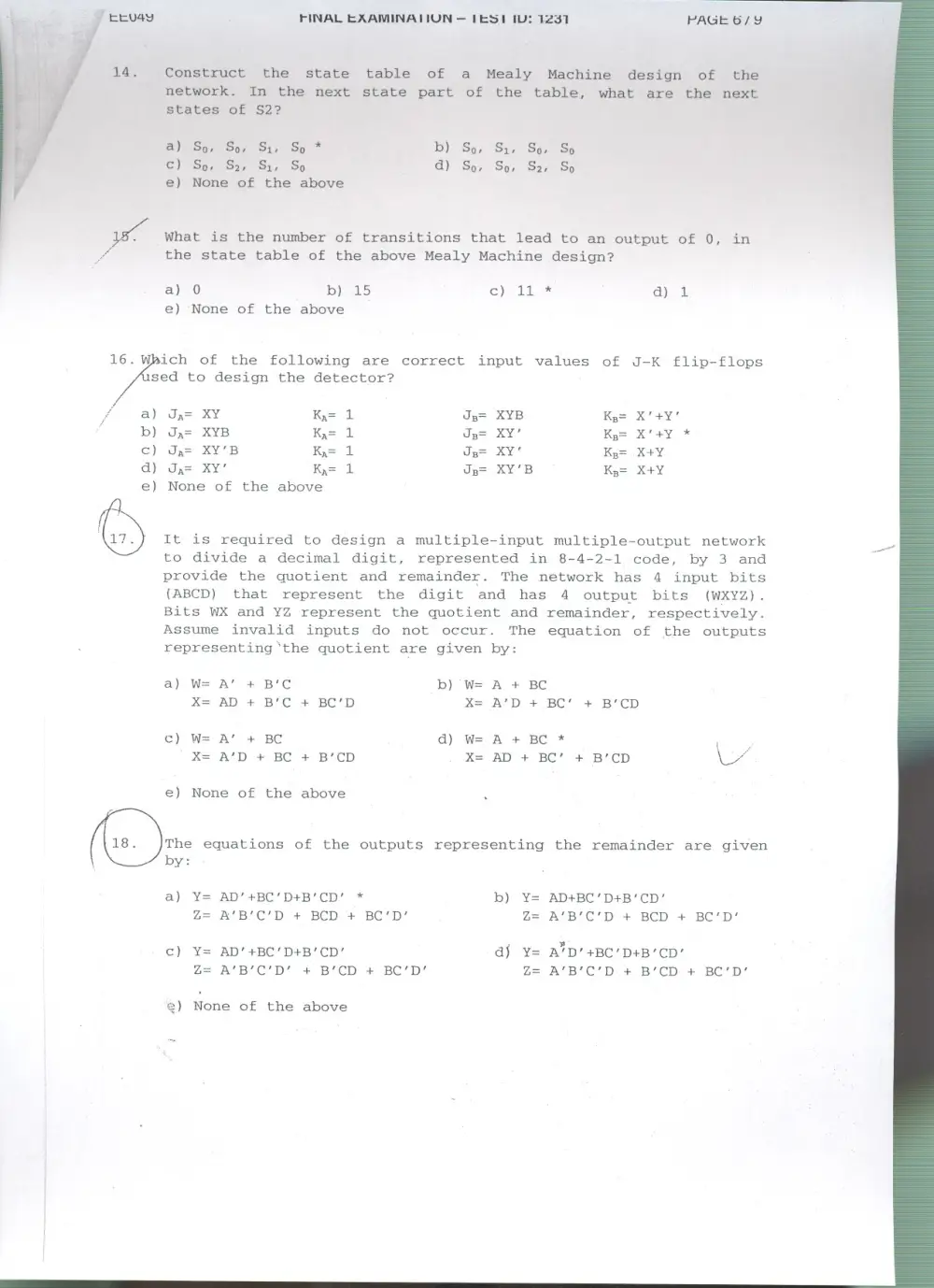
14.
Construct
the
state
table
of
a
Mealy
Machine
design
of
the
network.
In
the
next
state
part
of
the
table,
what
are
the
next
states
of 52?
a) So, So, Sl, So *
C) So, S2' Sl' So
e) None
of the above
b)
So,
Sl'
d)
So,
So,
What
is the number
of transitions
that
lead
to an output
of 0, in
the
state
table
of the above
Mealy
Machine
design?
a) 0
b) 15
e) None of the above
c) 11 *
d) 1
16.~iCh
of
the following are correct
input
~~sed
to design the detector?
,/
a)
JA= XY
KA= 1
JB= XYB
.'
b)
JA=
XYB
KA= 1
JB=
XY'
c)
JA= XY'B
KA= 1
JB= XY'
d)
JA= XY'
KA= 1
JB= XY'B
e)
None of the above
(0
values
of J-K
flip-flops
It
is
required
to
design
a multiple-input
multiple-output
network
to divide a decimal digit, represented in 8-4-2-1.code, by
3
and
provide the quotient and
remainde~. The network has
4 input bits
(ABCD)
that represent the digit and has 4 outpu.tbits
(WXYZ).
Bits WX and
YZ represent the quotient and remainder, respectively.
Assume
invalid
inputs
do
not
occur.
The
equation
of
the
outputs
representing\the
quotient
are
given
by:
e) None
of the
above
~The
equations
of
the
outputs
representing
the
remainder
are
given
(~bY:
KB= X'+Y'
KB= X' +Y
*
KB=
X+Y
KB= X+Y
a)
W= A'
+ B'C
b)
W= A + BC
X= AD + B'C
+ BC'D
X= A'D
+ BC'
+ B'CD
c)
W= A'
+ BC
d)
W= A + BC *
\J/
X= A'D
+ BC + B'CD
X= AD + BC'
+ B'CD
a)
Y= AD'+BC'D+B'CD'
*
b)
Y= AD+BC'D+B'CD'
Z= A'B'C'D
+ BCD + BC'D'
Z= A'B'C'D
+ BCD + BC'D'
dl
....
c)
Y= AD'+BC'D+B'CD'
Y= A'D'+BC'D+B'CD'
Z= A'B'C'D'
+ B'CD
+ BC'D'
z=
A'B'C'D
+ B'CD
+ BC'D'
) None of
the
above
I
\
,iI\
I!
t:.t:.U4~
FINALEXAMINATION- TEST ID:1231
PAGE 7/9
For
the
following three problems
consider
design an iterative network where each cell
Mealy state diagram below.
the
it
is
required
to
i is represented by the
19.
The output
(Zi) of each cell detects the following input pattern
when it occurs at any 4 adjacent cells in the network.
a)
1110
or
1101
c)
1011
or
1101
*
e) None
of
the above
b)
1010
or
d)
1011
or
1101
1110
20.
Using
a binary
state
assignment
(i.e.,
So= 000,
S1= 001),
then
the
next-cell
outputs
are
given
by:
b)
ai+1= aici'
+
Xiaici
bi+1= xi'aici
+ XibiCi'
Ci+l= xi'ai'ci +
Xiai'Ci'
d)
ai+1=
aiCi
+
xiai' Ci
bi+1=
Xi' aici
+
XibiCi'
Ci+1=
Xiai' Ci
+
Xi' aiCi'
21.
The
output
Zi of each
cell
is given
by:
a)
Zi= Xiaici
+ XibiCi
c)
Zi=
xi'aici
+ XibiCI
e)
None
of
the
above
b)
zi=
Xi' aici
+ Xibi' Ci
d)
Zi=
xiaici
+
XibiCi'
*
22.
A
sequential network with
one
constructed.
Its output Z is
occurs. The network does not
set is as follows:
input X and one output Z is to be
1 if an
input sequence 101 or
011
reset. A
typical input-output data
x=
0 1 0 1 0 0 1 0 1 1 0 1 0 0 1 1 1
z=
0 0 0 1 0 0 0 0 1 1 0 1 0 0 0 1 0
a)
ai+l= aiCi, + XiaiCi
bi+).
= xi'ai'ci + XibiCi+ Xiaici
Ci+l= Xiaici + Xi'aiCi'+
Xi' aiCi ,
c) ai+l= aiCi, + Xiai'Ci
*
bi+1= Xi'
ai'
Ci
+ XibiCi' + Xiaici
Ci+1= XiaiCi + xiai'Ci, + Xi'aiCi'
e) None
of
the above
EE049
FINAL EXAMINATION-,TEST ID: 1231
PAGE
8/9
The
state graph
of
a Mealy machine
to
realize
the above network
is
given by:
(a)
(c)
*
(e)
None of the above
(b)
(d)
23.
Using a
binary
state assignment
(i.e.,
So=
000,
S1=
001,
S2=
010),
then
the
input
equations
of
three
D
flip-flops (A,
B,
and
C)
realizing
the
above
sequential
network
are
given
by:
a)
c)
e)
--
DA = X' C
b )DA
= X' C '
DB = X'A'
+ XBC'
+ X'BC'
DB = XA'
+ X'B'C'
+ X'BC'
Dc = X
Dc = X'
DA = X' C '
*
d)
DA = XC'
DB = XA + X'C
+ XBC'
DB = X'A
+ XBC + X'C
Dc = X
Dc = X'
None
of
the
above
.-11..1"\
a.;..n.MIVII I'81"\ I IVI..
-
~
I
I..,.
I"""
. n
L-v I V
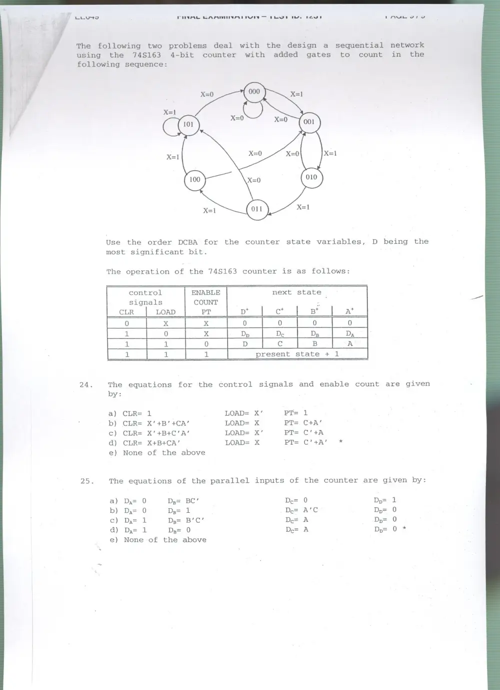
The
following two problems deal with
the design a
sequential network
using
the
745163
4-bit
counter
with
added
gates
to
count
in
the
following sequence:
Use the order
DCBA
for the counter
state variables,
D being the
most
significant
bit.
24.
The equations for the control signals and enable count are given
by:
The
operation
of
the 745163
counter
is as
follows:
control
ENABLE
I
next
state
signals
COUNT
.-
CLR
LOAD
PT
D+
C+
B+
A+
0
X
X
0
0
0
0
1
0
X
DD
Dc
DB
DA
1
1
0
D
C
B
A
1
1
1
present state + 1
a) CLR=
1
LOAD=
X'
PT.= 1
b)CLR=
X' +B' +CA'
LOAD=
X
PT=
C+A'
c) CLR=
X'+B+C'A'
LOAD=
X'
PT=
C' +A
d) CLR=
X+B+CA'
LOAD=
X
PT=
C'+A'
*
e) None
of the
above
25.
The
equations
of
the parallel
inputs
of
the
counter
are
given
by:
a) DA= 0
DB= BC'
Dc= 0
DD= 1
b) DA= 0
DB= 1
Dc=
A' C
DD= 0
c) DA= 1
DB= B'C'
Dc= A
DD= 0
d) DA= 1
DB= 0
Dc= A
DD=O*
e) None of the above