
EECE 320 Problems For Final, Fall 2008
American University of Beirut · Digital Systems Design · 10 pages · Prof. Mohammad Mansour



More EECE 320 files
- Final · Fall 2011Final examView
- Final · Fall 2010Final examView
- Final with Solutions · Fall 2009Final exam · with solutionView
- Final · Fall 2005Final examView
- Final with Solution · Fall 2005Final exam · with solutionView
- Homework 2 and 3 · Summer 2016HomeworkView
- Homework 1 · Summer 2016HomeworkView
- Homework 1 · Fall 2016HomeworkView
Show the text of this final exam
Prof. M. Mansour
Page 1 of 10
Sample Problems
Problem 1: K-Map Minimization [6 points]
Minimize the following 5-variable Boolean function:
F = ΣA,B,C,D,E(4, 5, 6, 7, 12, 14, 16, 20, 21, 24, 26, 27, 31) + d(0, 11, 19, 22, 30)
The minimum SOP of F is:
______________________________________________________________________
Prof. M. Mansour
Page 2 of 10
Sample Problems
Problem 2: Design Using Multiplexers [6 points]
Design the function below using a 4-input multiplexer with control variables A and B and additional
gates.
F = A’B’C’D’ + A’B’C’D + A’B’CD + A’BC’D + A’BCD’ +
AB’C’D’ + AB’C’D + ABC’D’ + ABC’D
Solution:
Prof. M. Mansour
Page 3 of 10
Sample Problems
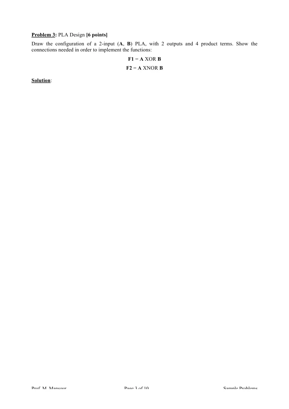
Problem 3: PLA Design [6 points]
Draw the configuration of a 2-input (A, B) PLA, with 2 outputs and 4 product terms. Show the
connections needed in order to implement the functions:
F1 = A XOR B
F2 = A XNOR B
Solution:
Prof. M. Mansour
Page 4 of 10
Sample Problems
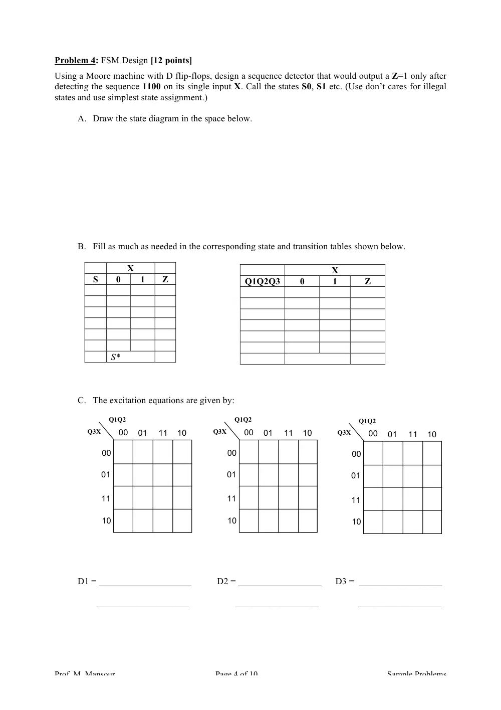
Problem 4: FSM Design [12 points]
Using a Moore machine with D flip-flops, design a sequence detector that would output a Z=1 only after
detecting the sequence 1100 on its single input X. Call the states S0, S1 etc. (Use don’t cares for illegal
states and use simplest state assignment.)
A. Draw the state diagram in the space below.
B. Fill as much as needed in the corresponding state and transition tables shown below.
X
S
0
1
Z
S*
C. The excitation equations are given by:
D1 = ____________________ D2 = __________________ D3 = __________________
____________________ __________________ __________________
X
Q1Q2Q3
0
1
Z
Q3X
Q1Q2
00
01
11
10
00
01
11
10
Q3X
Q1Q2
00
01
11
10
00
01
11
10
Q3X
Q1Q2
00
01
11
10
00
01
11
10
Prof. M. Mansour
Page 5 of 10
Sample Problems
Problem 5: FSM Design Using VHDL [12 points]
Write a VHDL code to implement the sequence detector of the previous question.
Prof. M. Mansour
Page 6 of 10
Sample Problems
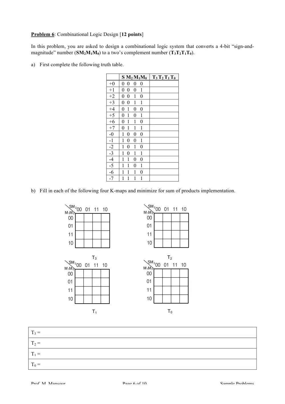
Problem 6: Combinational Logic Design [12 points]
In this problem, you are asked to design a combinational logic system that converts a 4-bit “sign-and-
magnitude” number (SM2M1M0) to a two’s complement number (T3T2T1T0).
a) First complete the following truth table.
S M2 M1M0 T3 T2 T1 T0
+0
0 0 0 0
+1
0 0 0 1
+2
0 0 1 0
+3
0 0 1 1
+4
0 1 0 0
+5
0 1 0 1
+6
0 1 1 0
+7
0 1 1 1
-0
1 0 0 0
-1
1 0 0 1
-2
1 0 1 0
-3
1 0 1 1
-4
1 1 0 0
-5
1 1 0 1
-6
1 1 1 0
-7
1 1 1 1
b) Fill in each of the following four K-maps and minimize for sum of products implementation.
T3 =
T2 =
T1 =
T0 =
T3
T2
T1
T0
Prof. M. Mansour
Page 7 of 10
Sample Problems
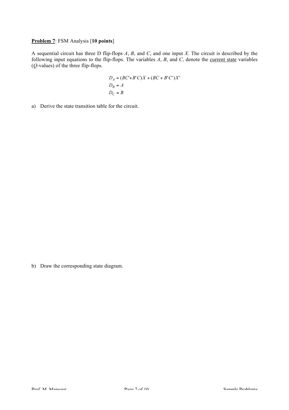
Problem 7: FSM Analysis [10 points]
A sequential circuit has three D flip-flops A, B, and C, and one input X. The circuit is described by the
following input equations to the flip-flops. The variables A, B, and C, denote the current state variables
(Q-values) of the three flip-flops.
a) Derive the state transition table for the circuit.
b) Draw the corresponding state diagram.
Prof. M. Mansour
Page 8 of 10
Sample Problems
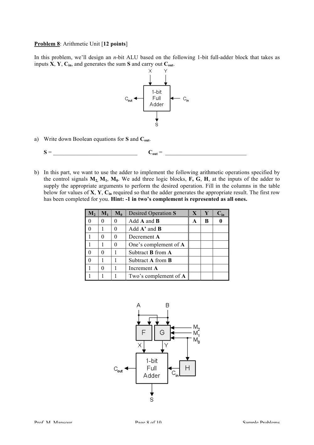
Problem 8: Arithmetic Unit [12 points]
In this problem, we’ll design an n-bit ALU based on the following 1-bit full-adder block that takes as
inputs X, Y, Cin, and generates the sum S and carry out Cout.
a) Write down Boolean equations for S and Cout.
S = _____________________________
Cout = ____________________________
b) In this part, we want to use the adder to implement the following arithmetic operations specified by
the control signals M2, M1, M0. We add three logic blocks, F, G, H, at the inputs of the adder to
supply the appropriate arguments to perform the desired operation. Fill in the columns in the table
below for values of X, Y, Cin required so that the adder generates the appropriate result. The first row
has been completed for you. Hint: -1 in two’s complement is represented as all ones.
M2 M1
M0
Desired Operation S
X
Y
Cin
0
0
0
Add A and B
A
B
0
0
1
0
Add A’ and B
1
0
0
Decrement A
1
1
0
One’s complement of A
0
0
1
Subtract B from A
0
1
1
Subtract A from B
1
0
1
Increment A
1
1
1
Two’s complement of A
Prof. M. Mansour
Page 9 of 10
Sample Problems
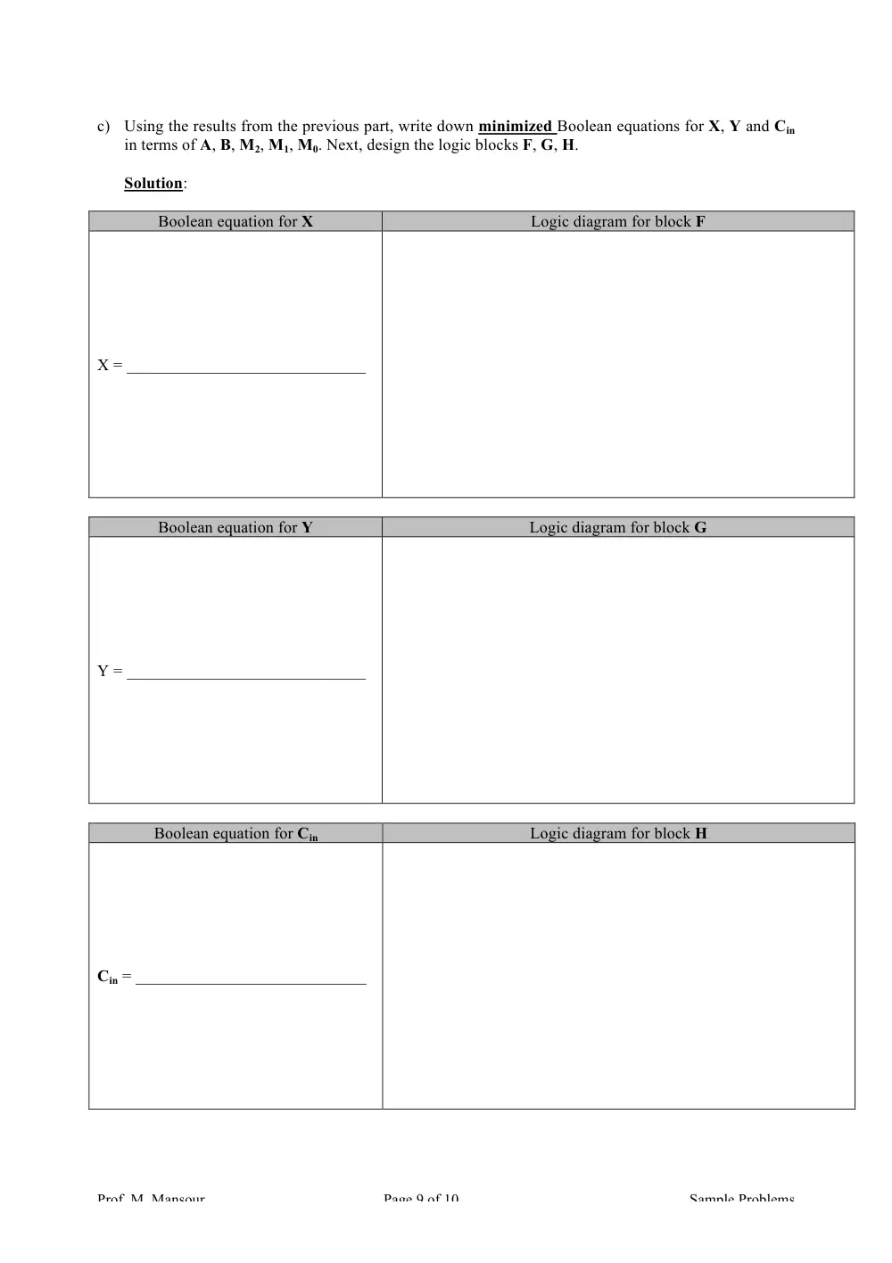
c) Using the results from the previous part, write down minimized Boolean equations for X, Y and Cin
in terms of A, B, M2, M1, M0. Next, design the logic blocks F, G, H.
Solution:
Boolean equation for X
Logic diagram for block F
X = _____________________________
Boolean equation for Y
Logic diagram for block G
Y = _____________________________
Boolean equation for Cin
Logic diagram for block H
Cin = ____________________________
Prof. M. Mansour
Page 10 of 10
Sample Problems
Problem 9: Arithmetic Unit [20 points]
The following questions are independent.
a) The following memories are specified by the number of words times the number of bits per
word. How many address lines, input-output data lines are needed in each case, and how many
bytes does each memory store: [4 points]
Memory
Address lines
Input-Output lines
Number of bytes
16K x 8
256K x 16
64M x 32
2G x 8
b) A 64K x 16 RAM chip is designed in such a way that its cell array is square, i.e., it contains an
equal number of bit-cells per row and column. A row decoder is used to select a row, and a
column decoder is used to select the appropriate set of columns. Determine the following:
i.
Number of bits in the cell array. [1 point]
ii. Size of the row decoder and the number of AND gates required to implement it. [3
points]
iii. Size of column decoder and the number of AND gates required to implement it. [3
points]
iv. If the input address (076400)8 is applied to the chip, which row and column selection
lines are enabled. Give your answers in decimal. [2 points]
c) A 256Mb DRAM chip has a 4-bit data input bus and a 4-bit output data bus. Also, it has equal
length row and column addresses. How many address pins does the DRAM have? [4 points]
d) How many 128K x 16 DRAM chips are needed to provide memory capacity of 1M bytes? How
many address lines are required to access 1M bytes? How many of these lines are connected to
the address inputs of all chips? [3 points]