
EECE 320 Final, Fall 2011
American University of Beirut · Digital Systems Design · 11 pages · Dr. Youssef Nasser


Showing the first 10 of 11 pages. Download the PDF to see all of it.
More EECE 320 files
- Final · Fall 2010Final examView
- Final with Solutions · Fall 2009Final exam · with solutionView
- Problems For Final · Fall 2008Final examView
- Final · Fall 2005Final examView
- Final with Solution · Fall 2005Final exam · with solutionView
- Homework 2 and 3 · Summer 2016HomeworkView
- Homework 1 · Summer 2016HomeworkView
- Homework 1 · Fall 2016HomeworkView
Show the text of this final exam
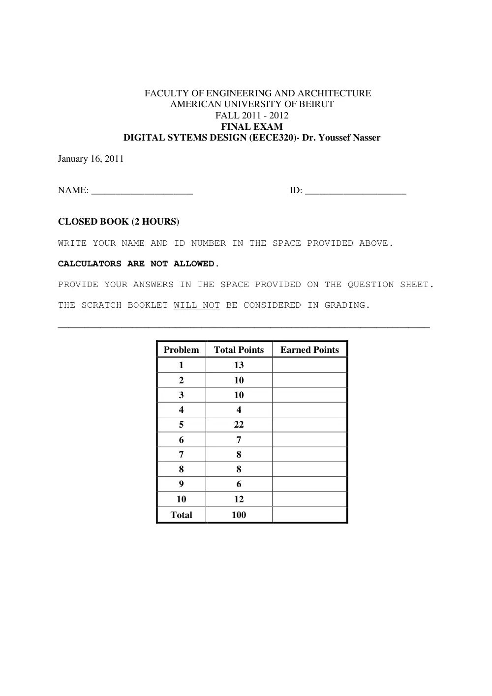
FACULTY OF ENGINEERING AND ARCHITECTURE
AMERICAN UNIVERSITY OF BEIRUT
FALL 2011 - 2012
FINAL EXAM
DIGITAL SYTEMS DESIGN (EECE320)- Dr. Youssef Nasser
January 16, 2011
NAME: _____________________
ID: _____________________
CLOSED BOOK (2 HOURS)
WRITE YOUR NAME AND ID NUMBER IN THE SPACE PROVIDED ABOVE.
CALCULATORS ARE NOT ALLOWED.
PROVIDE YOUR ANSWERS IN THE SPACE PROVIDED ON THE QUESTION SHEET.
THE SCRATCH BOOKLET WILL NOT BE CONSIDERED IN GRADING.
______________________________________________________________________
Problem
Total Points
Earned Points
1
13
2
10
3
10
4
4
5
22
6
7
7
8
8
8
9
6
10
12
Total
100
EECE 320
FINAL EXAM
2/11
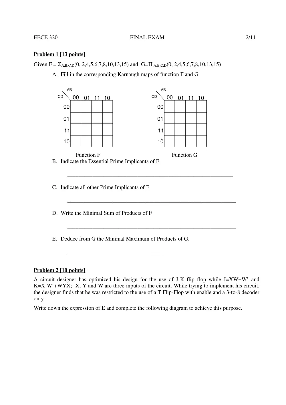
Problem 1 [13 points]
Given F = ΣA,B,C,D(0, 2,4,5,6,7,8,10,13,15) and G=Π A,B,C,D(0, 2,4,5,6,7,8,10,13,15)
A. Fill in the corresponding Karnaugh maps of function F and G
Function F Function G
B. Indicate the Essential Prime Implicants of F
___________________________________________________________
C. Indicate all other Prime Implicants of F
____________________________________________________________
D. Write the Minimal Sum of Products of F
____________________________________________________________
E. Deduce from G the Minimal Maximum of Products of G.
____________________________________________________________
Problem 2 [10 points]
A circuit designer has optimized his design for the use of J-K flip flop while J=XW+W’ and
K=X’W’+WYX; X, Y and W are three inputs of the circuit. While trying to implement his circuit,
the designer finds that he was restricted to the use of a T Flip-Flop with enable and a 3-to-8 decoder
only.
Write down the expression of E and complete the following diagram to achieve this purpose.
CD
AB
00 01 11 10
00
01
11
10
CD
AB
00 01 11 10
00
01
11
10
EECE 320
FINAL EXAM
3/11
E = _______________________________
Problem 3 [10 points]
1. We would like to analyze the following clocked synchronous state machine.
J2
K2
clk
X
Y
Z
T
rstn
rstn
z1
z2
A. Write the next state equations for z1 and z2.
z1* = ____________________________________
z2* = ____________________________________
B. Draw the transition/output table.
XY
z2 z1
00
01
11
10
ZT
0 0
0 1
1 1
1 0
z2* z1*
E
Q
QN
T
EECE 320
FINAL EXAM
4/11
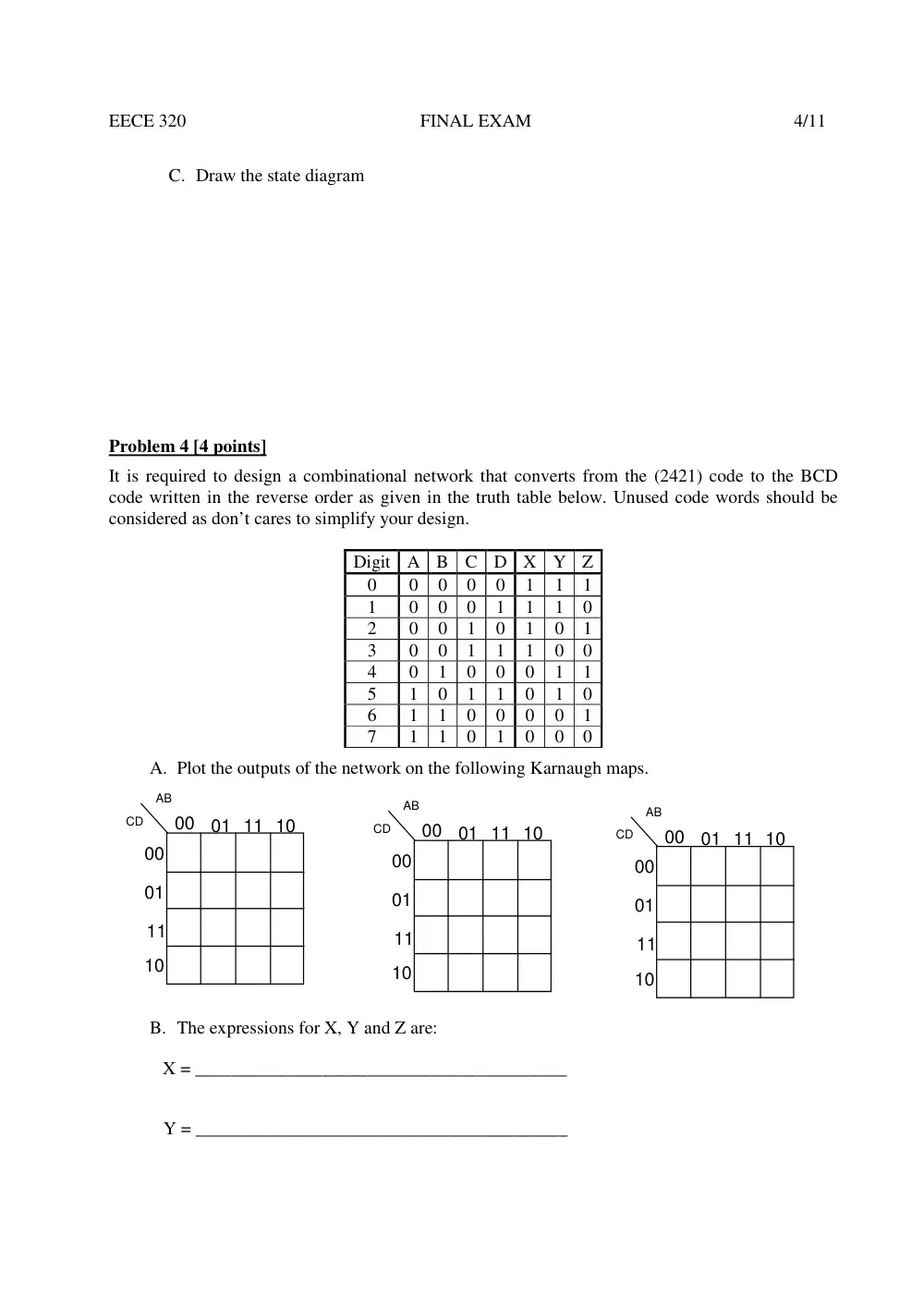
C. Draw the state diagram
Problem 4 [4 points]
It is required to design a combinational network that converts from the (2421) code to the BCD
code written in the reverse order as given in the truth table below. Unused code words should be
considered as don’t cares to simplify your design.
Digit A B C D X Y Z
0
0
0
0
0
1
1
1
1
0
0
0
1
1
1
0
2
0
0
1
0
1
0
1
3
0
0
1
1
1
0
0
4
0
1
0
0
0
1
1
5
1
0
1
1
0
1
0
6
1
1
0
0
0
0
1
7
1
1
0
1
0
0
0
A. Plot the outputs of the network on the following Karnaugh maps.
B. The expressions for X, Y and Z are:
X = _________________________________________
Y = _________________________________________
CD
AB
00 01 11 10
00
01
11
10
CD
AB
00 01 11 10
00
01
11
10
CD
AB
00 01 11 10
00
01
11
10
EECE 320
FINAL EXAM
5/11
Z = _________________________________________
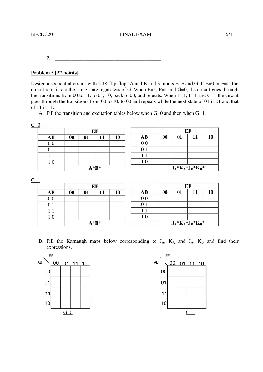
Problem 5 [22 points]
Design a sequential circuit with 2 JK flip-flops A and B and 3 inputs E, F and G. If E=0 or F=0, the
circuit remains in the same state regardless of G. When E=1, F=1 and G=0, the circuit goes through
the transitions from 00 to 11, to 01, 10, back to 00, and repeats. When E=1, F=1 and G=1 the circuit
goes through the transitions from 00 to 10, to 00 and repeats while the next state of 01 is 01 and that
of 11 is 11.
A. Fill the transition and excitation tables below when G=0 and then when G=1.
G=0
EF
AB
00
01
11
10
0 0
0 1
1 1
1 0
A*B*
G=1
EF
AB
00
01
11
10
0 0
0 1
1 1
1 0
A*B*
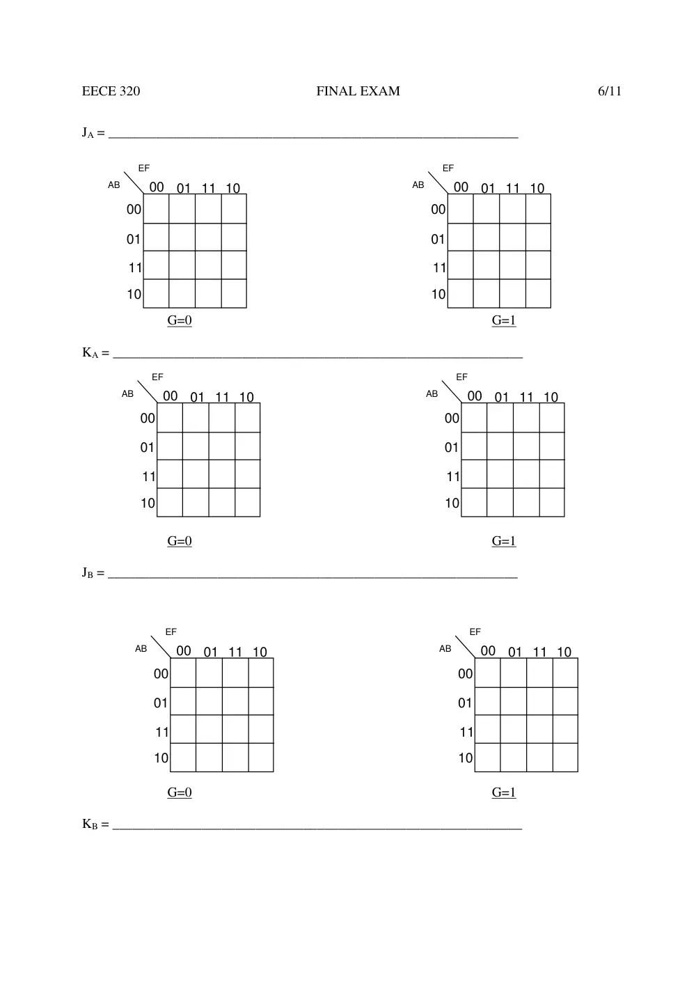
B. Fill the Karnaugh maps below corresponding to JA, KA and JA, KB and find their
expressions.
G=0
G=1
EF
AB
00
01
11
10
0 0
0 1
1 1
1 0
JA*KA*JB*KB*
EF
AB
00
01
11
10
0 0
0 1
1 1
1 0
JA*KA*JB*KB*
AB
EF
00 01 11 10
00
01
11
10
AB
EF
00 01 11 10
00
01
11
10
EECE 320
FINAL EXAM
6/11
JA = ____________________________________________________________
G=0
G=1
KA = ____________________________________________________________
G=0
G=1
JB = ____________________________________________________________
G=0
G=1
KB = ____________________________________________________________
AB
EF
00 01 11 10
00
01
11
10
AB
EF
00 01 11 10
00
01
11
10
AB
EF
00 01 11 10
00
01
11
10
AB
EF
00 01 11 10
00
01
11
10
AB
EF
00 01 11 10
00
01
11
10
AB
EF
00 01 11 10
00
01
11
10
EECE 320
FINAL EXAM
7/11
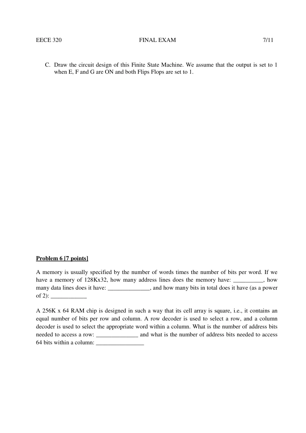
C. Draw the circuit design of this Finite State Machine. We assume that the output is set to 1
when E, F and G are ON and both Flips Flops are set to 1.
Problem 6 [7 points]
A memory is usually specified by the number of words times the number of bits per word. If we
have a memory of 128Kx32, how many address lines does the memory have: __________, how
many data lines does it have: ______________, and how many bits in total does it have (as a power
of 2): ____________
A 256K x 64 RAM chip is designed in such a way that its cell array is square, i.e., it contains an
equal number of bits per row and column. A row decoder is used to select a row, and a column
decoder is used to select the appropriate word within a column. What is the number of address bits
needed to access a row: ______________ and what is the number of address bits needed to access
64 bits within a column: ________________
EECE 320
FINAL EXAM
8/11
Problem 7 [8 points]
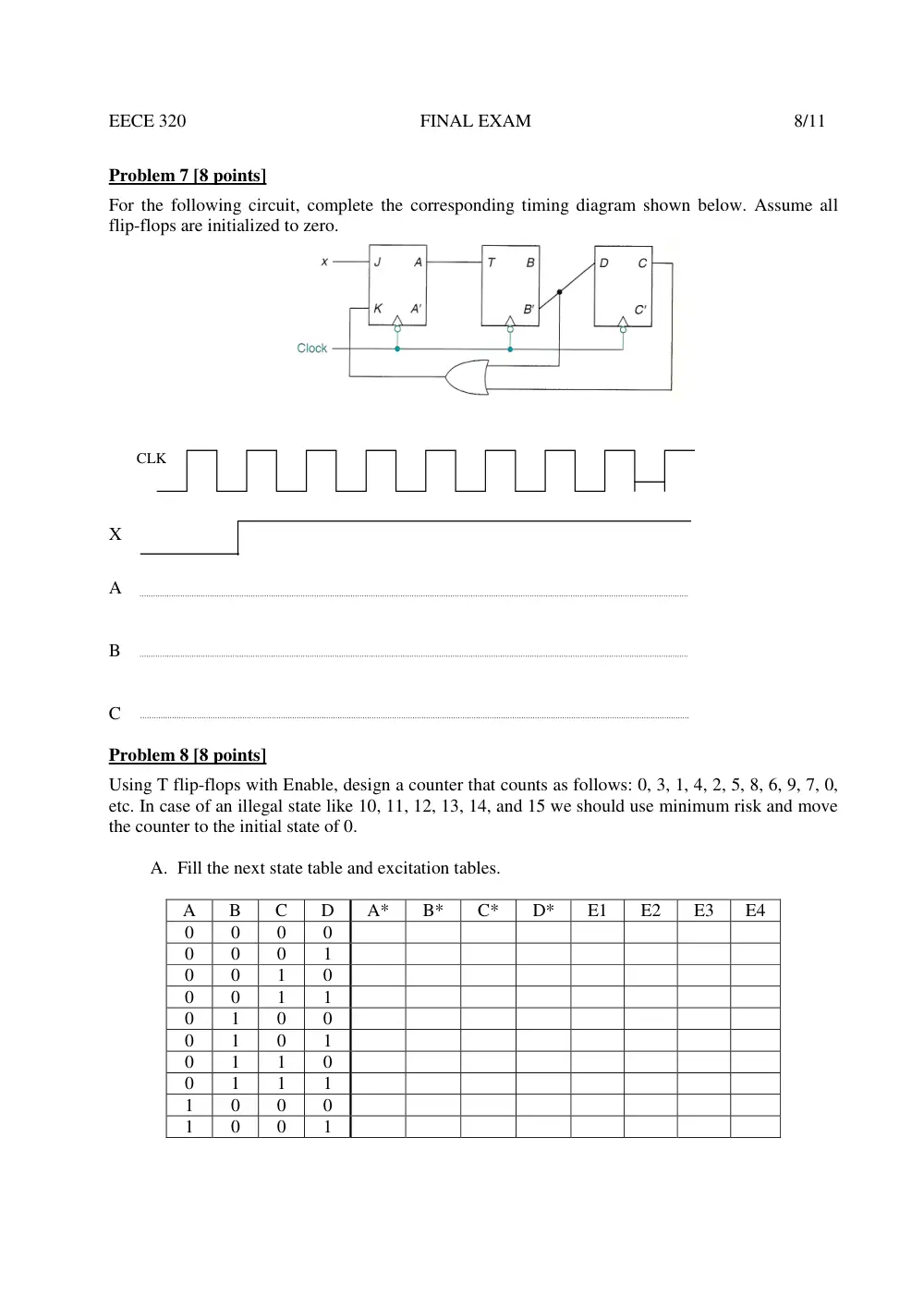
For the following circuit, complete the corresponding timing diagram shown below. Assume all
flip-flops are initialized to zero.
X
A
B
C
Problem 8 [8 points]
Using T flip-flops with Enable, design a counter that counts as follows: 0, 3, 1, 4, 2, 5, 8, 6, 9, 7, 0,
etc. In case of an illegal state like 10, 11, 12, 13, 14, and 15 we should use minimum risk and move
the counter to the initial state of 0.
A. Fill the next state table and excitation tables.
A
B
C
D
A*
B*
C*
D*
E1
E2
E3
E4
0
0
0
0
0
0
0
1
0
0
1
0
0
0
1
1
0
1
0
0
0
1
0
1
0
1
1
0
0
1
1
1
1
0
0
0
1
0
0
1
CLK
EECE 320
FINAL EXAM
9/11
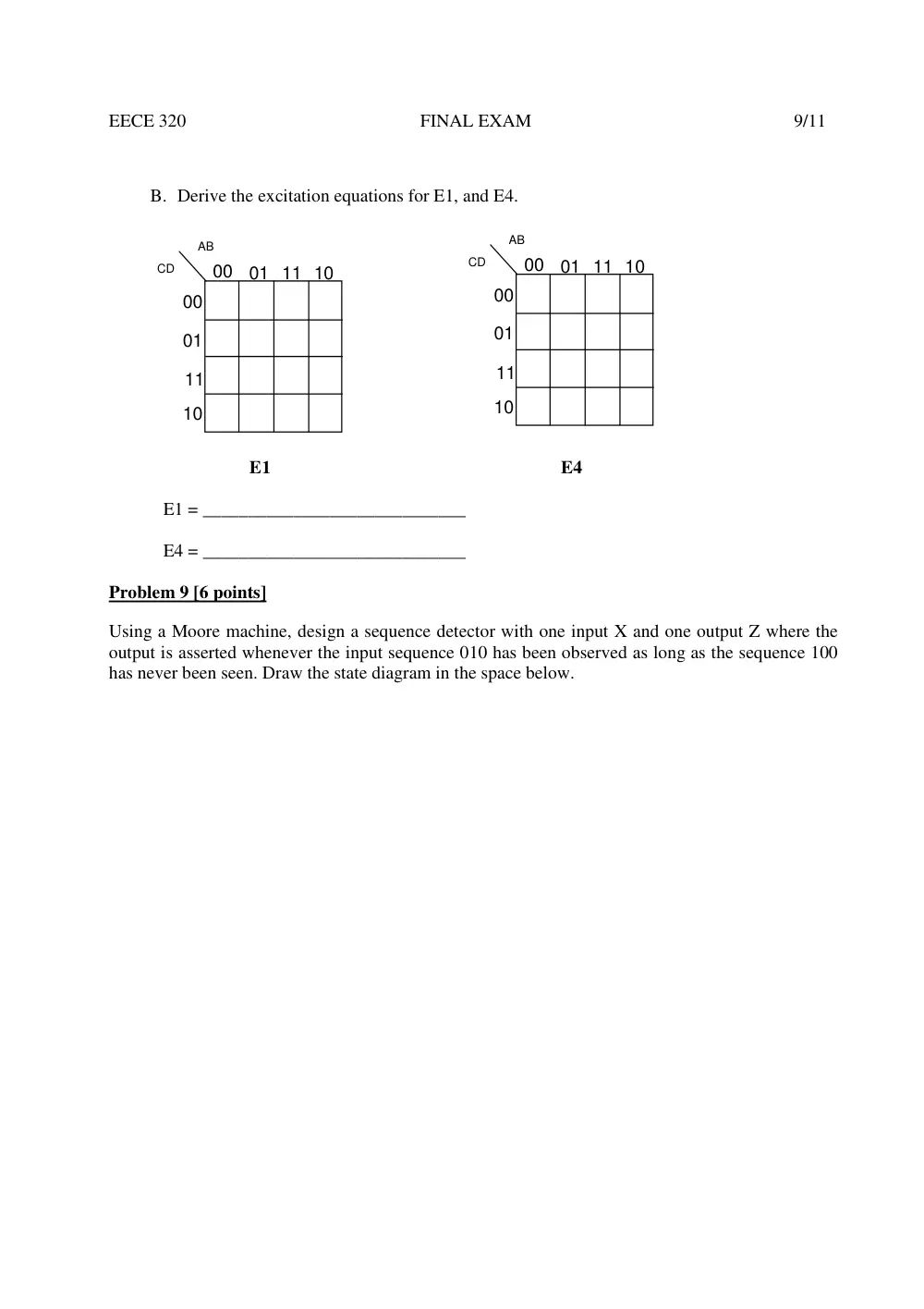
B. Derive the excitation equations for E1, and E4.
E1 E4
E1 = _____________________________
E4 = _____________________________
Problem 9 [6 points]
Using a Moore machine, design a sequence detector with one input X and one output Z where the
output is asserted whenever the input sequence 010 has been observed as long as the sequence 100
has never been seen. Draw the state diagram in the space below.
CD
AB
00 01 11 10
00
01
11
10
CD
AB
00 01 11 10
00
01
11
10
EECE 320
FINAL EXAM
10/11
Problem 10 ( 12 points)
Write a VHDL code to implement a 3-bits Gray counter (equivalent to Gray decoder).
EECE 320
FINAL EXAM
11/11