
MECH 430 Homework Lecture Assignment, Spring 2017
American University of Beirut · Instrumentation and Measurements · 17 pages


Showing the first 10 of 17 pages. Download the PDF to see all of it.
More MECH 430 files
Show the text of this lab
HOMEWORK ONE
MECH 43O
FEBRUARY 26, 2017
SARA ALAWIEH
201601126
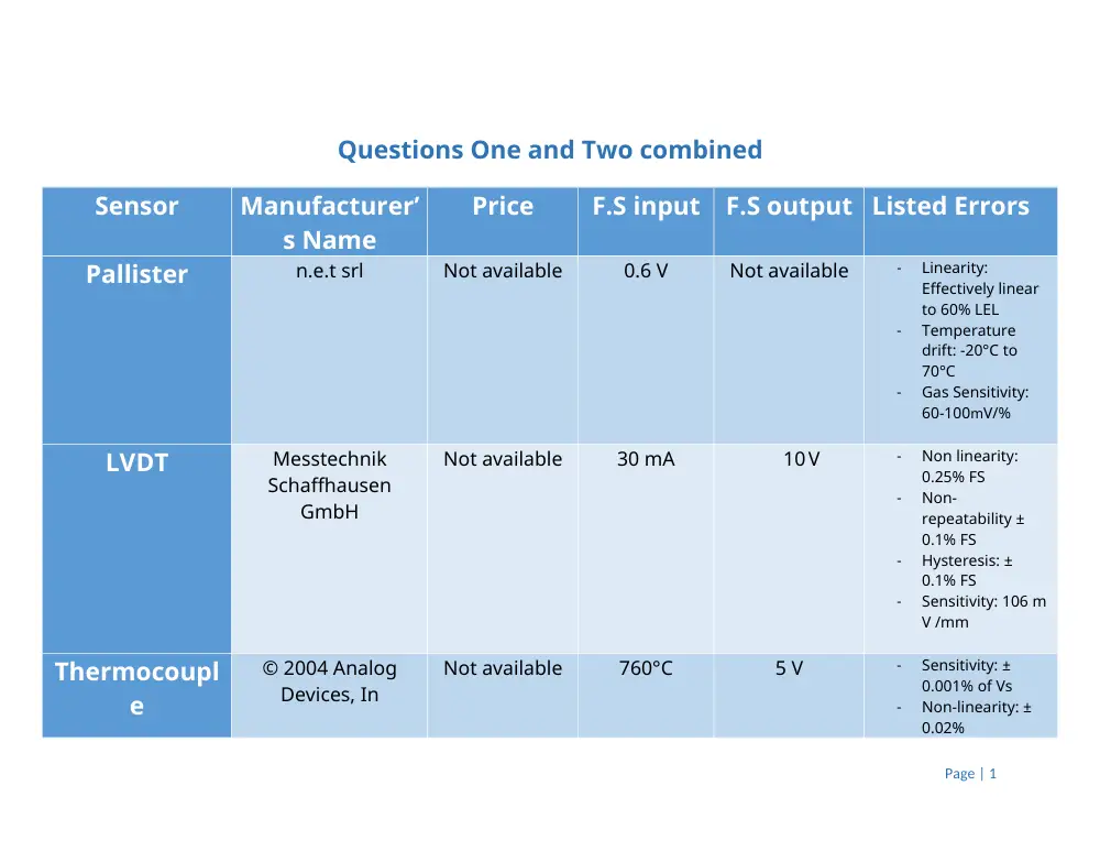
Questions One and Two combined
Page | 1
Sensor
Manufacturer’
s Name
Price
F.S input
F.S output Listed Errors
Pallister
n.e.t srl
Not available
0.6 V
Not available
-
Linearity:
Effectively linear
to 60% LEL
-
Temperature
drift: -20°C to
70°C
-
Gas Sensitivity:
60-100mV/%
LVDT
Messtechnik
Schaffhausen
GmbH
Not available
30 mA
10V
-
Non linearity:
0.25% FS
-
Non-
repeatability ±
0.1% FS
-
Hysteresis: ±
0.1% FS
-
Sensitivity: 106 m
V /mm
Thermocoupl
e
© 2004 Analog
Devices, In
Not available
760°C
5 V
-
Sensitivity: ±
0.001% of Vs
-
Non-linearity: ±
0.02%
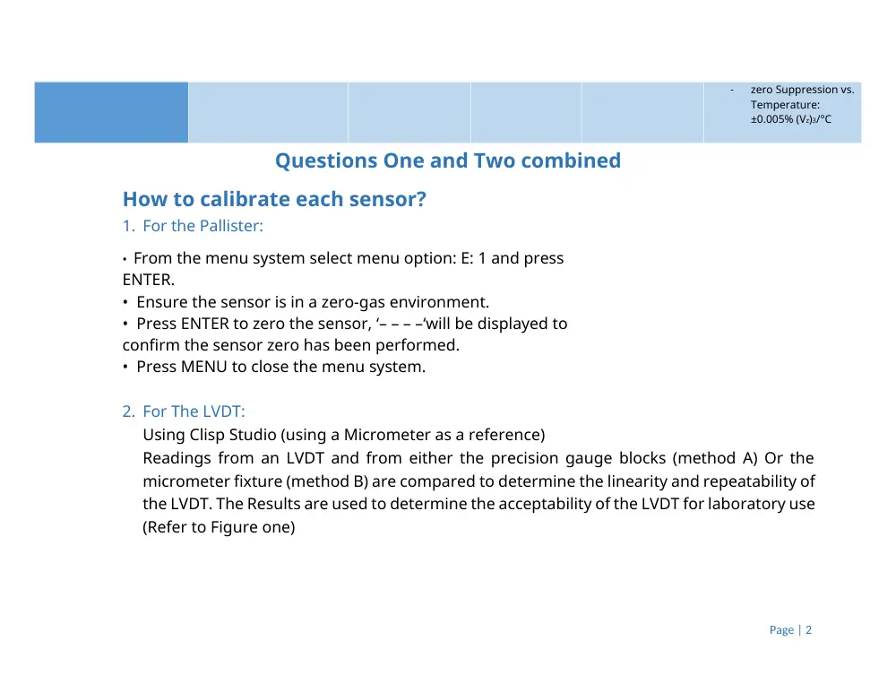
Questions One and Two combined
How to calibrate each sensor?
1. For the Pallister:
• From the menu system select menu option: E: 1 and press
ENTER.
• Ensure the sensor is in a zero-gas environment.
• Press ENTER to zero the sensor, ‘– – – –‘will be displayed to
confirm the sensor zero has been performed.
• Press MENU to close the menu system.
2. For The LVDT:
Using Clisp Studio (using a Micrometer as a reference)
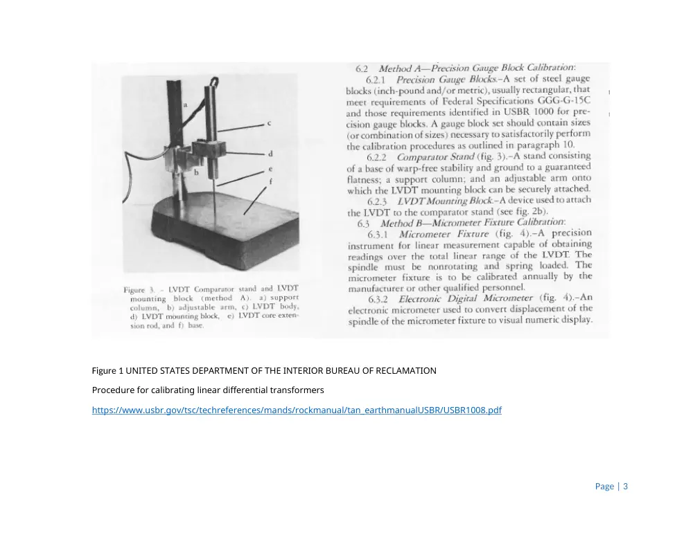
Readings from an LVDT and from either the precision gauge blocks (method A) Or the
micrometer fixture (method B) are compared to determine the linearity and repeatability of
the LVDT. The Results are used to determine the acceptability of the LVDT for laboratory use
(Refer to Figure one)
Page | 2
-
zero Suppression vs.
Temperature:
±0.005% (Vz)3/°C
Page | 3
Figure 1 UNITED STATES DEPARTMENT OF THE INTERIOR BUREAU OF RECLAMATION
Procedure for calibrating linear differential transformers
https://www.usbr.gov/tsc/techreferences/mands/rockmanual/tan_earthmanualUSBR/USBR1008.pdf
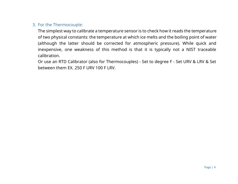
3. For the Thermocouple:
The simplest way to calibrate a temperature sensor is to check how it reads the temperature
of two physical constants: the temperature at which ice melts and the boiling point of water
(although the latter should be corrected for atmospheric pressure). While quick and
inexpensive, one weakness of this method is that it is typically not a NIST traceable
calibration.
Or use an RTD Calibrator (also for Thermocouples) - Set to degree F - Set URV & LRV & Set
between them EX. 250 F URV 100 F LRV.
Page | 4
Technical changes reserved -
Latest updates of data sheet always under www.burster.com
burster praezisionsmesstechnik gmbh & co kg . Tel. +49-7224-6450 . Fax 64588
Talstr. 1-5 . DE-76593 Gernsbach . www.burster.com . info@burster.com
8739 EN
Code:
8739 EN
Delivery:
ex stock
Warranty:
24 months
IN-LINE amplifier
Displacement sensor
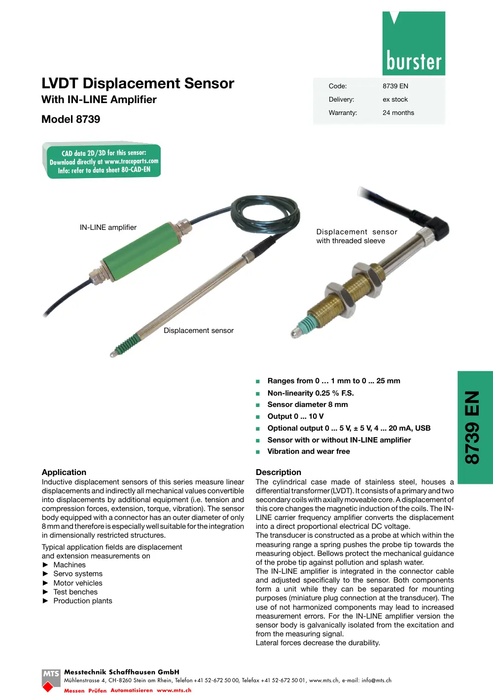
LVDT Displacement Sensor
With IN-LINE Amplifier
Model 8739
Application
Inductive displacement sensors of this series measure linear
displacements and indirectly all mechanical values convertible
into displacements by additional equipment (i.e. tension and
compression forces, extension, torque, vibration). The sensor
body equipped with a connector has an outer diameter of only
8 mm and therefore is especially well suitable for the integration
in dimensionally restricted structures.
Typical application fields are displacement
and extension measurements on
► Machines
► Servo systems
► Motor vehicles
► Test benches
► Production plants
Description
The cylindrical case made of stainless steel, houses a
differential transformer (LVDT). It consists of a primary and two
secondary coils with axially moveable core. A displacement of
this core changes the magnetic induction of the coils. The IN-
LINE carrier frequency amplifier converts the displacement
into a direct proportional electrical DC voltage.
The transducer is constructed as a probe at which within the
measuring range a spring pushes the probe tip towards the
measuring object. Bellows protect the mechanical guidance
of the probe tip against pollution and splash water.
The IN-LINE amplifier is integrated in the connector cable
and adjusted specifically to the sensor. Both components
form a unit while they can be separated for mounting
purposes (miniature plug connection at the transducer). The
use of not harmonized components may lead to increased
measurement errors. For the IN-LINE amplifier version the
sensor body is galvanically isolated from the excitation and
from the measuring signal.
Lateral forces decrease the durability.
Q
Ranges from 0 … 1 mm to 0 ... 25 mm
Q
Non-linearity 0.25 % F.S.
Q
Sensor diameter 8 mm
Q
Output 0 ... 10 V
Q Optional output 0 ... 5 V, ± 5 V, 4 ... 20 mA, USB
Q
Sensor with or without IN-LINE amplifier
Q Vibration and wear free
Displacement sensor
with threaded sleeve
MTS
Messtechnik Schaffhausen GmbH
Mühlenstrasse 4, CH-8260 Stein am Rhein, Telefon +41 52-672 50 00, Telefax +41 52-672 50 01, www.mts.ch, e-mail: info@mts.ch
Messen Prüfen Automatisieren www.mts.ch
1738-008739EN-5672-011516
Technical changes reserved -
Latest updates of data sheet always under www.burster.com
burster praezisionsmesstechnik gmbh & co kg . Tel. +49-7224-6450 . Fax 64588
Talstr. 1-5 . DE-76593 Gernsbach . www.burster.com . info@burster.com
8739 EN - 2
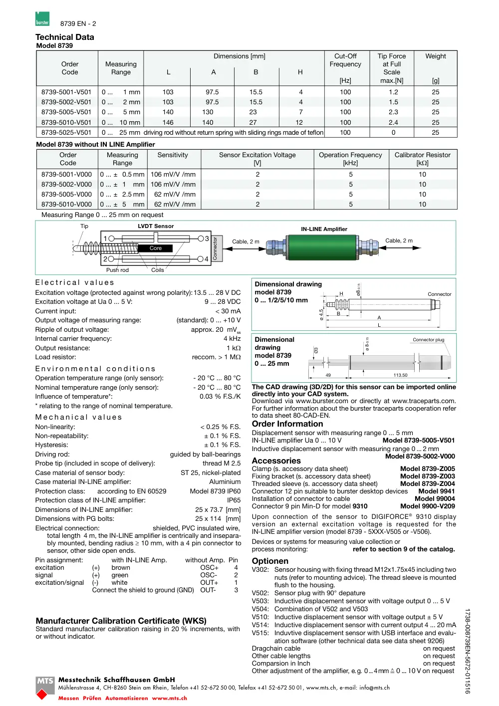
Technical Data
E l e c t r i c a l v a l u e s
Excitation voltage (protected against wrong polarity): 13.5 ... 28 V DC
Excitation voltage at Ua 0 ... 5 V:
9 ... 28 VDC
Current input:
< 30 mA
Output voltage of measuring range:
(standard): 0 ... +10 V
Ripple of output voltage:
approx. 20 mVss
Internal carrier frequency:
4 kHz
Output resistance:
1 kW
Load resistor:
reccom. > 1 MW
E n v i r o n m e n t a l c o n d i t i o n s
Operation temperature range (only sensor):
- 20 °C ... 80 °C
Nominal temperature range (only sensor):
- 20 °C ... 80 °C
Influence of temperature*:
0.03 % F.S./K
* relating to the range of nominal temperature.
M e c h a n i c a l v a l u e s
Non-linearity:
< 0.25 % F.S.
Non-repeatability:
± 0.1 % F.S.
Hysteresis:
± 0.1 % F.S.
Driving rod:
guided by ball-bearings
Probe tip (included in scope of delivery):
thread M 2.5
Case material of sensor body:
ST 25, nickel-plated
Case material IN-LINE amplifier:
Aluminium
Protection class:
according to EN 60529
Model 8739 IP60
Protection class of IN-LINE amplifier:
IP65
Dimensions of IN-LINE amplifier:
25 x 73.7 [mm]
Dimensions with PG bolts:
25 x 114 [mm]
Electrical connection:
shielded, PVC insulated wire,
total length 4 m, the IN-LINE amplifier is centrically and insepara-
bly mounted, bending radius ≥ 10 mm, with a 4 pin connector to
sensor, other side open ends.
Pin assignment:
with IN-LINE Amp.
without Amp. Pin
excitation
(+)
brown
OSC+
4
signal
(+)
green
OSC-
2
excitation/signal
(-)
white
OUT+
1
Connect the shield to ground (GND) OUT-
3
B
ø8-0.15
ø 4.5
A
L
H
Connector
Dimensional drawing
model 8739
0 ... 1/2/5/10 mm
IN-LINE Amplifier
LVDT Sensor
Cable, 2 m
Push rod
1
2
3
4
Coils
Tip
Core
Connector
Cable, 2 m
The CAD drawing (3D/2D) for this sensor can be imported online
directly into your CAD system.
Download via www.burster.com or directly at www.traceparts.com.
For further information about the burster traceparts cooperation refer
to data sheet 80-CAD-EN.
Order Information
Displacement sensor with measuring range 0 ... 5 mm
IN-LINE amplifier Ua 0 ... 10 V
Model 8739-5005-V501
Inductive displacement sensor with measuring range 0 ... 2 mm
Model 8739-5002-V000
Accessories
Clamp (s. accessory data sheet)
Model 8739-Z005
Fixing bracket (s. accessory data sheet)
Model 8739-Z003
Threaded sleeve (s. accessory data sheet)
Model 8739-Z004
Connector 12 pin suitable to burster desktop devices
Model 9941
Installation of connector to cable
Model 99004
Connector 9 pin Min-D for model 9310
Model 9900-V209
Upon connection of the sensor to DIGIFORCE® 9310 display
version an external excitation voltage is requested for the
IN-LINE amplifier version (model 8739 - 5XXX-V505 or -V506).
Devices or systems for measuring value collection or
process monitoring:
refer to section 9 of the catalog.
Optionen
V302: Sensor housing with fixing thread M12x1.75x45 including two
nuts (refer to mounting advice). The thread sleeve is mounted
flush to the housing.
V502: Sensor plug with 90° depature
V503: Inductive displacement sensor with voltage output 0 ... 5 V
V504: Combination of V502 and V503
V510: Inductive displacement sensor with voltage output ± 5 V
V514: Inductive displacement sensor with current output 4 ... 20 mA
V515: Induvtive displacement sensor with USB interface and evalu-
ation software (other technical data see data sheet 9206)
Dragchain cable
on request
Other cable lengths
on request
Comparsion in Inch
on request
Other adjustment of the amplifier, e. g. 0 ... 4 mm ≙ 0 ... 10 V on request
Dimensional
drawing
model 8739
0 ... 25 mm
Manufacturer Calibration Certificate (WKS)
Standard manufacturer calibration raising in 20 % increments, with
or without indicator.
Model 8739 without IN LINE Amplifier
8739-5001-V000
0 ... ± 0.5 mm 106 mV/V /mm
2
5
10
8739-5002-V000
0 ... ± 1 mm 106 mV/V /mm
2
5
10
8739-5005-V000
0 ... ± 2.5 mm
62 mV/V /mm
2
5
10
8739-5010-V000
0 ... ± 5 mm
62 mV/V /mm
2
5
10
Measuring Range 0 ... 25 mm on request
Order
Measuring
Sensitivity
Sensor Excitation Voltage
Operation Frequency
Calibrator Resistor
Code
Range
[V]
[kHz]
[kW]
8739-5001-V501
0 ...
1 mm
103
97.5
15.5
4
100
1.2
25
8739-5002-V501
0 ...
2 mm
103
97.5
15.5
4
100
1.5
25
8739-5005-V501
0 ...
5 mm
140
130
23
7
100
2.3
25
8739-5010-V501
0 ... 10 mm
146
140
27
12
100
2.4
25
8739-5025-V501
0 ... 25 mm driving rod without return spring with sliding rings made of teflon
100
0
25
Model 8739
Dimensions [mm]
Cut-Off
Tip Force
Weight
Order
Measuring
Frequency
at Full
Code
Range
L
A
B
H
Scale
[Hz]
max.[N]
[g]
Connector plug
113.50
49
Ø3
ø 8-0.15
MTS
Messtechnik Schaffhausen GmbH
Mühlenstrasse 4, CH-8260 Stein am Rhein, Telefon +41 52-672 50 00, Telefax +41 52-672 50 01, www.mts.ch, e-mail: info@mts.ch
Messen Prüfen Automatisieren www.mts.ch
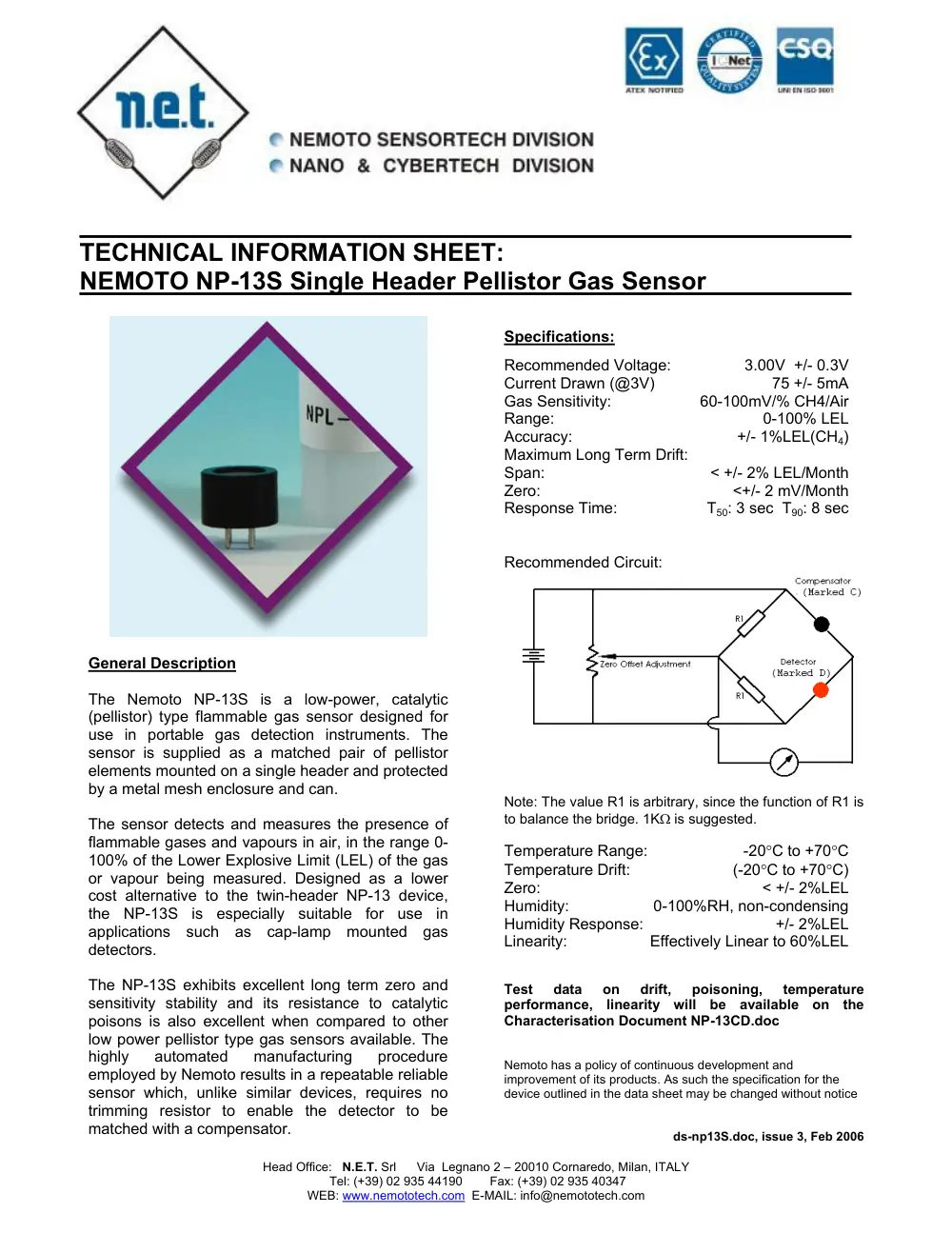
TECHNICAL INFORMATION SHEET:
NEMOTO NP-13S Single Header Pellistor Gas Sensor
Specifications:
Recommended Voltage:
3.00V +/- 0.3V
Current Drawn (@3V)
75 +/- 5mA
Gas Sensitivity:
60-100mV/% CH4/Air
Range:
0-100% LEL
Accuracy:
+/- 1%LEL(CH4)
Maximum Long Term Drift:
Span:
< +/- 2% LEL/Month
Zero:
<+/- 2 mV/Month
Response Time:
T50: 3 sec T90: 8 sec
Recommended Circuit:
General Description
The Nemoto NP-13S is a low-power, catalytic
(pellistor) type flammable gas sensor designed for
use in portable gas detection instruments. The
sensor is supplied as a matched pair of pellistor
elements mounted on a single header and protected
by a metal mesh enclosure and can.
Note: The value R1 is arbitrary, since the function of R1 is
to balance the bridge. 1KΩ is suggested.
The sensor detects and measures the presence of
flammable gases and vapours in air, in the range 0-
100% of the Lower Explosive Limit (LEL) of the gas
or vapour being measured. Designed as a lower
cost alternative to the twin-header NP-13 device,
the NP-13S is especially suitable for use in
applications such as cap-lamp mounted gas
detectors.
Temperature Range:
-20°C to +70°C
Temperature Drift:
(-20°C to +70°C)
Zero:
< +/- 2%LEL
Humidity:
0-100%RH, non-condensing
Humidity Response:
+/- 2%LEL
L
inearity:
Effectively Linear to 60%LEL
The NP-13S exhibits excellent long term zero and
sensitivity stability and its resistance to catalytic
poisons is also excellent when compared to other
low power pellistor type gas sensors available. The
highly
automated
manufacturing
procedure
employed by Nemoto results in a repeatable reliable
sensor which, unlike similar devices, requires no
trimming resistor to enable the detector to be
matched with a compensator.
Test
data
on
drift,
poisoning,
temperature
performance, linearity will be available on the
Characterisation Document NP-13CD.doc
Nemoto has a policy of continuous development and
improvement of its products. As such the specification for the
device outlined in the data sheet may be changed without notice
ds-np13S.doc, issue 3, Feb 2006
Head Office: N.E.T. Srl
Via Legnano 2 – 20010 Cornaredo, Milan, ITALY
Tel: (+39) 02 935 44190 Fax: (+39) 02 935 40347
WEB: www.nemototech.com E-MAIL: info@nemototech.com
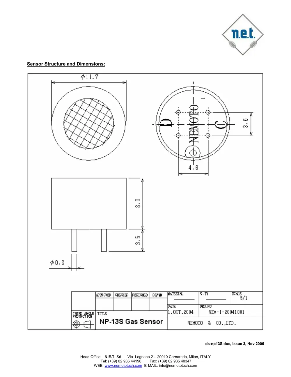
Sensor Structure and Dimensions:
ds-np13S.doc, issue 3, Nov 2006
Head Office: N.E.T. Srl
Via Legnano 2 – 20010 Cornaredo, Milan, ITALY
Tel: (+39) 02 935 44190 Fax: (+39) 02 935 40347
WEB: www.nemototech.com E-MAIL: info@nemototech.com
Isolated, Linearized Thermocouple Input
7B47
Rev. 0
Information furnished by Analog Devices is believed to be accurate and reliable.
However, no responsibility is assumed by Analog Devices for its use, nor for any
infringements of patents or other rights of third parties that may result from its use.
Specifications subject to change without notice. No license is granted by implication
or otherwise under any patent or patent rights of Analog Devices. Trademarks and
registered trademarks are the property of their respective companies.
One Technology Way, P.O. Box 9106, Norwood, MA 02062-9106, U.S.A.
Tel: 781.329.4700
www.analog.com
Fax: 781.326.8703
© 2004 Analog Devices, Inc. All rights reserved.
FEATURES
Interfaces, amplifies and filters input voltages from a J, K, T,
E, R, S, B or N-type thermocouple.
Module provides a precision output of either +1 V to +5 V or
0 V to +10 V, linear with input temperature.
All 7B47 series modules are mix-and-match and Hot
Swappable.
APPLICATIONS
Industrial signal conditioning
Industrial signal isolation
Industrial signal filtering
PRODUCT OVERVIEW
The 7B Series of signal conditioners feature small size, low cost
and a wide output voltage range for a variety of applications
including process control and factory-floor environments. The
single-channel 7B modules accept inputs from a range of
transducers and are fully rated over the extended -40oC to
+85oC industrial temperature range. All 7B Series modules are
rated for a nominal power supply input of +24 VDC; and, for
maximum flexibility, they will accept supply voltages in the +14
VDC to +35 VDC range. The input modules, with the exception
of the 7B21, provide a high-level output voltage that is factory
configured for either the +1 V to +5 V or 0 V to +10 V range.
The 7B21 is a unity gain, isolated input module with an
input/output range of +10V. Output modules are available that
provide either isolated process current or isolated bipolar
voltage output. Model 7B39 converts either a +1 V to +5 V input
to a 4 to 20 mA output or a 0 V to +10 V input to a 0-20 mA
output. The input/output ranges of the 7B39 are factory
configured. The 7B22 is a unity gain module that provides an
isolated +10V output signal. All modules have a universal pin-
out and may be readily hot-swapped under full power without
disrupting field wiring. Each module accepts analog transducer
signals and transfers them to a process control or factory data
collection system without the inherent noise, non-linearity, drift
and extraneous voltages which frequently accompany the
signals.
FUNCTIONAL BLOCK DIAGRAM
Figure 1. 7B47 Functional Block Diagram
The modules feature a maximum nonlinearity of +0.02% and
are factory calibrated to guarantee a maximum accuracy
specification of +0.1%.
The 7B Series offers up to 1500 V rms continuous common
mode voltage isolation and 120 V rms of field wiring input
protection. The power supplies necessary to drive each of the
individual module’s input circuitry are internally isolated,
enabling the 7B Series modules to offer true channel-to-channel
isolation of the input signals.
The modules directly accept analog signals from
thermocouples, RTDs, current loop powered transmitters, and
other process control signals. The 7B Series modules amplify,
linearize, isolate, protect and convert the transducer output
signals to standardized analog inputs for high-level analog I/O
subsystems. The 7B Series Subsystem consists of 19-inch rack-
compatible hardware (model AC 1363), with universal
mounting backplane and a family of plug-in (up to 16 per
backplane) input and output signal conditioning modules. Four-
, eight-, and sixteen-channel backplanes are available. Each
backplane incorporates screw terminals for easy power
connections and field wiring, and includes a 25-pin D-type
connector for interfacing the high-level single-ended voltage
outputs to the user’s equipment. Gold-plated sockets are
provided on each channel of the backplane to ensure the
reliability of each module’s electrical connection.
7B47
Rev. 0 | Page 2 of 8
GENERAL DESCRIPTION
The 7B47 is a single-channel signal conditioning module that
interfaces, amplifies and filters input voltages from a J, K, T, E, R,
S, B, or N-type thermocouple and provides an isolated and
protected precision output of either +1V to +5V or 0 to +10 V,
linear with input temperature. High accuracy internal cold
junction compensation and a predictable upscale open circuit
indication provide a complete signal conditioning solution. To
accurately measure low level signals in electrically noisy
environments, 1500 V rms of galvanic transformer-based
isolation with a common mode rejection (CMR) of 160 of 160
dB @ 50/60 Hz and a normal mode rejection (NMR) of 60 dB @
50/60 Hz are provided. Rated to operate with a nominal +24
VDC supply, Model 7B47 is mix-and-match and hot-swappable
with other 7B Series input modules, so it can be inserted or
removed from any socket in the same backplane without
disturbing system power.
The three input pins of model 7B47 are fully protected up to
120 V rms line voltages. A one-pole 3 Hz filter preconditions the
thermocouple signal prior to amplification, provided by a low
drift input amplifier. Cold junction compensation (CJC) is
implemented using a thermistor temperature sensor embedded
under the input screw terminal block on a 7B Series backplane.
A voltage reference source acts to offset the thermocouple
signal in accordance with the specified lower bound on the
input temperature range. A current source provides the upscale
open circuit indication. Amplitude modulation is used to
implement transformer isolation (1500) V rms input-to-output
and power). Isolated front-end circuitry power is supplied by a
DC/DC converter. The output section contains a demodulator,
linearizer. A two-pole low pass filter (-3 dB @ 3 Hz), a buffer
amplifier and a power oscillator. The two-pole output filter and
subsequent buffer ensures that a low noise, low impedance
(<1Ω) signal is available at the output to drive loads down to 2
kΩ .
Figure 2
7B47
Rev. 0 | Page 3 of 8
7B47 Models Available
Model
Input Type
Input Range
Output Range
Accuracy1
(Typical)
Accuracy1
(Maximum)
7B47-J-01-1
Type J
0°C to +760°C (+32°F to +1400°F)
+1 V to +5 V
±0.15% Span
±0.38% Span
7B47-J-01-2
Type J
0°C to +760°C (+32°F to +1400°F)
0 V to +10 V
±0.13% Span
±0.32% Span
7B47-J-02-1
Type J
-100°C to +300°C (-148°F to +572°F)
+1 V to +5 V
±0.16% Span
±0.35% Span
7B47-J-02-2
Type J
-100°C to +300°C (-148°F to +572°F)
0 V to +10 V
±0.14% Span
±0.30% Span
7B47-K-03-1
Type K
0°C to +1300°C (+32°F to +2372°F)
+1 V to +5 V
±0.15% Span
±0.35% Span
7B47-K-03-2
Type K
0°C to +1300°C (+32°F to +2372°F)
0 V to +10 V
±0.15% Span
±0.32% Span
7B47-K-04-1
Type K
0°C to +600°C (-148°F to +1112°F)
+1 V to +5 V
±0.09% Span
±0.20% Span
7B47-K-04-2
Type K
0°C to +600°C (-148°F to +1112°F)
0 V to +10 V
±0.08% Span
±0.18% Span
7B47-T-05-1
Type T
0°C to +400°C (+32°F to +752°F)
+1 V to +5 V
±0.24% Span
±0.05% Span
7B47-T-05-2
Type T
0°C to +400°C (+32°F to +752°F)
0 V to +10 V
±0.19% Span
±0.38% Span
7B47-T-06-1
Type T
-100°C to +200°C (-148°F to +392°F)
+1 V to +5 V
±0.29% Span
±0.57% Span
7B47-T-06-2
Type T
-100°C to +200°C (-148°F to +392°F)
0 V to +10 V
±0.25% Span
±0.47% Span
7B47-E-07-1
Type E
0°C to +900°C (+32°F to +1652°F)
+1 V to +5 V
±0.18% Span
±0.41% Span
7B47-E-07-2
Type E
0°C to +900°C (+32°F to +1652°F)
0 V to +10 V
±0.15% Span
±0.34% Span
7B47-R-08-1
Type R
+500°C to +1750°C (+932°F to +3182°F)
+1 V to +5 V
±0.29% Span
±0.36% Span
7B47-R-08-2
Type R
+500°C to +1750°C (+932°F to +3182°F)
0 V to +10 V
±0.25% Span
±0.30% Span
7B47-S-09-1
Type S
+700°C to +1750°C (+1292°F to +3182°F)
+1 V to +5 V
±0.13% Span
±0.31% Span
7B47-S-09-2
Type S
+700°C to +1750°C (+1292°F to +3182°F)
0 V to +10 V
±0.11% Span
±0.25% Span
7B47-B-10-1
Type B
+800°C to +1800°C (+1472°F to +3272°F)
+1 V to +5 V
±0.19% Span
±0.41% Span
7B47-B-10-2
Type B
+800°C to +1800°C (+1472°F to +3272°F)
0 V to +10 V
±0.17% Span
±0.35% Span
7B47-N-11-1
Type N
+200°C to +1300°C (+392°F to +2372°F)
+1 V to +5 V
±0.14% Span
±0.31% Span
7B47-N-11-2
Type N
+200°C to +1300°C (+392°F to +2372°F)
0 V to +10 V
±0.09% Span
±0.27% Span
1 Accuracy includes the effects of repeatability, hysteresis and conformity. The CJC sensor accuracy should be added to the 7B47 module accuracy listed in these tables in order to
compute the overall system accuracy.
7B47
Rev. 0 | Page 4 of 8
7B47 Specifications
(typical @ +23°C ±5°C and Vs = +24 V dc)
Description
Model 7B47
Input Ranges
Thermocouple Types
J, K, T, E, R, S, B, N
Standard Temperature Ranges
Refer to Model Table
Custom Ranges
Not Available*
Output Range Options (RL > 2 kΩ)
+1 V to +5 V or 0 V to +10 V
Accuracy1
Initial @ +25°C
Refer to Model Table
Input Offset vs. Temperature
±0.5 µV/°C
Zero Suppression vs. Temperature
±0.005% (Vz)3/°C
Span vs. Temperature
±40 ppm/°C
Output Offset vs. Temperature
±0.002% Span/°C
Cold Junction Compensation
Accuracy4, over +5°C to +45°C ambient
±1.0°C, maximum
Input Bias Current
+25 nA
Input Resistance
Power ON
10 MΩ
Power OFF
30 kΩ, minimum
Output Noise
5 MHz Bandwidth
7 mV peak
10 Hz to 100 kHz Bandwidth
1 mV rms
0.1 Hz to 10 Hz Bandwidth
0.5 µV peak
Bandwidth, -3 dB
3 Hz
Output Rise Time, 10% to 90% Span
150 ms
Common-Mode Voltage (CMV)
Input-to-Output and Power
1500 V rms, continuous
Common Mode Rejection (CMR)
Input-to-Output and Power @ 50/60 Hz
160 dB
Normal Mode Rejection @ 50/60 Hz
60 dB
Input Protection
120 V rms, continuous
±35 V dc, continuous
Input Transient Protection
ANSI/IEEE C376.90.1-1989
IEEE-STD 472
IEC 255-4, Class II
Output Resistance
< 1 Ω
Voltage Output Protection
Continuous Short to Ground
Power Supply
Voltage Range, Operating
+14 V dc to +35 V dc
7B47
Rev. 0 | Page 5 of 8
Current
+25 mA, maximum
Sensitivity
±0.0001%/% of Vs
Mechanical Dimensions
1.663" x 2.11" x 0.563"
(42.24 mm x 53.6 mm x 14.3 mm)
Weight
60 grams
Environmental
Temperature Range
Operating
-40°C to +85°C
Storage
-40°C to +85°C
Relative Humidity, 24 hours
0 to 90% @ +60°C non-condensing
ESD Sensitivity
IEC 801-2, Level 2
RFI Susceptibility
±0.5% Span error @ 400 MHz, 5 Watt, 3 ft
Warm-up time required to meet specifications is approximately 10 minutes.
* Contact factory for OEM requirements.
1Includes the combined effects of repeatability, hysteresis, and nonlinearity.
2Nonlinearity is calculated using best-fit straight line method.
3When used with the CJC temperature sensor provided an each
channel of 7B Series backplanes.
Specifications subject to change without notice.
7B47
Rev. 0 | Page 6 of 8
PIN CONFIGURATIONS AND FUNCTIONAL DESCRIPTIONS
Figure 3 7B47 Input Field Connections
Table 1. Pin Function Descriptions—
Pin
No.
Input Module Function
Output Module Function
0
SENSOR INPUT
NOT USED
1
INPUT HIGH
OUTPUT HIGH
2
INPUT LOW
OUTPUT LOW
3
POWER SUPPLY (DC)
POWER SUPPLY (DC)
4
OUTPUT VOLTAGE
INPUT VOLTAGE
5
OUTPUT & POWER
COMMON
INPUT AND POWER
COMMON
Figure 4 . Model 7B Series Module, with pin-out assignments.
ESD CAUTION
ESD (electrostatic discharge) sensitive device. Electrostatic charges as high as 4000 V readily accumulate on the human
body and test equipment and can discharge without detection. Although this product features proprietary ESD
protection circuitry, permanent damage may occur on devices subjected to high energy electrostatic discharges.
Therefore, proper ESD precautions are recommended to avoid performance degradation or loss of functionality.
7B47
Rev. 0 | Page 7 of 8
OUTLINE DIMENSIONS
Figure 5. Outline Dimensions
7B47
Rev. 0 | Page 8 of 8
NOTES
© 2004 Analog Devices, Inc. All rights reserved. Trademarks and
registered trademarks are the property of their respective companies.
D05182-0-10/04(0)