
MECH 430 Notes 6, Spring 2014
American University of Beirut · Instrumentation and Measurements · 127 pages


Showing the first 10 of 127 pages. Download the PDF to see all of it.
More MECH 430 files
Show the text of this notes
Instrumentation & Measurements
MECH 430
MECH 430
Slide 1
Chapter 6
Signal
Conditioning
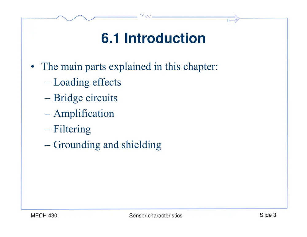
6.1 Introduction
MECH 430
Sensor characteristics
Slide 2
Physical
phenomenon
Sensor
(Transducer)
Signal
conditioning
Data
acquisition
PC
-Temperature
-Pressure
-Displacement
-Force
-Light
-Noise
-etc..
-Resistive
-Inductive
-Capacitive
-Light
-Magnetic
-Thermal
-Ultrasonic
etc..
-Amplification
-Linearization
-Excitation
-Isolation
-Averaging
-Filtering
-Modulation
etc..
-Analog
multiplexer
-Instrumentation
amplifier
-A/D, D/A
conversion
-Sample clock
-Trigger
-Analysis
-Feedback
control
-Display
6.1 Introduction
• The main parts explained in this chapter:
– Loading effects
– Bridge circuits
– Amplification
– Filtering
– Grounding and shielding
MECH 430
Sensor characteristics
Slide 3
6.3 Loading Error and
Impedance Matching
MECH 430
Sensor characteristics
Slide 4
MECH 430
Sensor characteristics
Slide 5
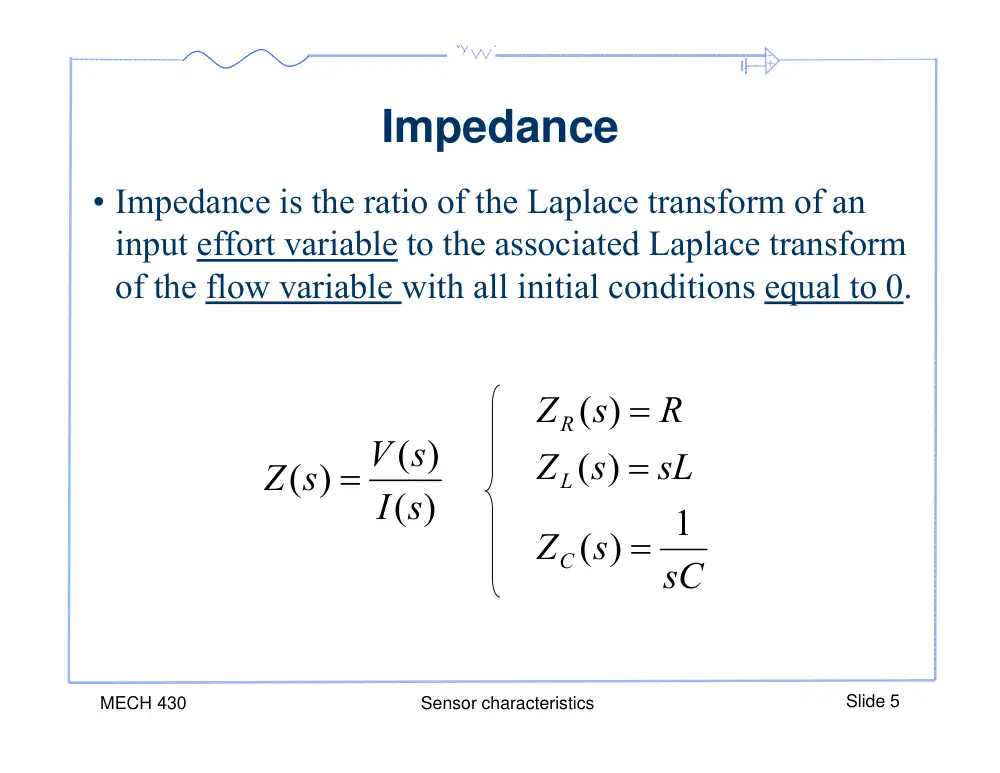
Impedance
• Impedance is the ratio of the Laplace transform of an
input effort variable to the associated Laplace transform
of the flow variable with all initial conditions equal to 0.
sC
s
Z
sL
s
Z
R
s
Z
C
L
R
1
)
(
)
(
)
(
( )
( )
( )
I s
V s
Z s
MECH 430
Sensor characteristics
Slide 6
Input Impedance
• The input impedance or load impedance of a circuit
or device is the opposition exhibited by its input
terminals to the flow of an alternating current of a
particular frequency as a result of resistance,
inductance, or capacitance.
• For example, an amplifier with 100,000 ohm input
impedance looks equivalent to a 100,000 ohm
resistor to the device driving it.
MECH 430
Sensor characteristics
Slide 7
Output Impedance
• The output impedance, source impedance, or
internal impedance of an electronic device is the
opposition exhibited by its output terminals to the
flow of an alternating current of a particular
frequency as a result of resistance, inductance, or
capacitance.
• For example, a preamplifier with 100Ω output
impedance means the output voltage signal appears
to be in series with a 100Ω resistor.
Loading Error
• Ideally, an instrument should not affect the
variable being measured.
• If it does, it will alter the variable being
measured
• Loading error is the difference between the
value of the measurand and the indicated value
by the instrument.
• Loading effects can be electrical, mechanical,
optical etc.
MECH 430
Sensor characteristics
Slide 8
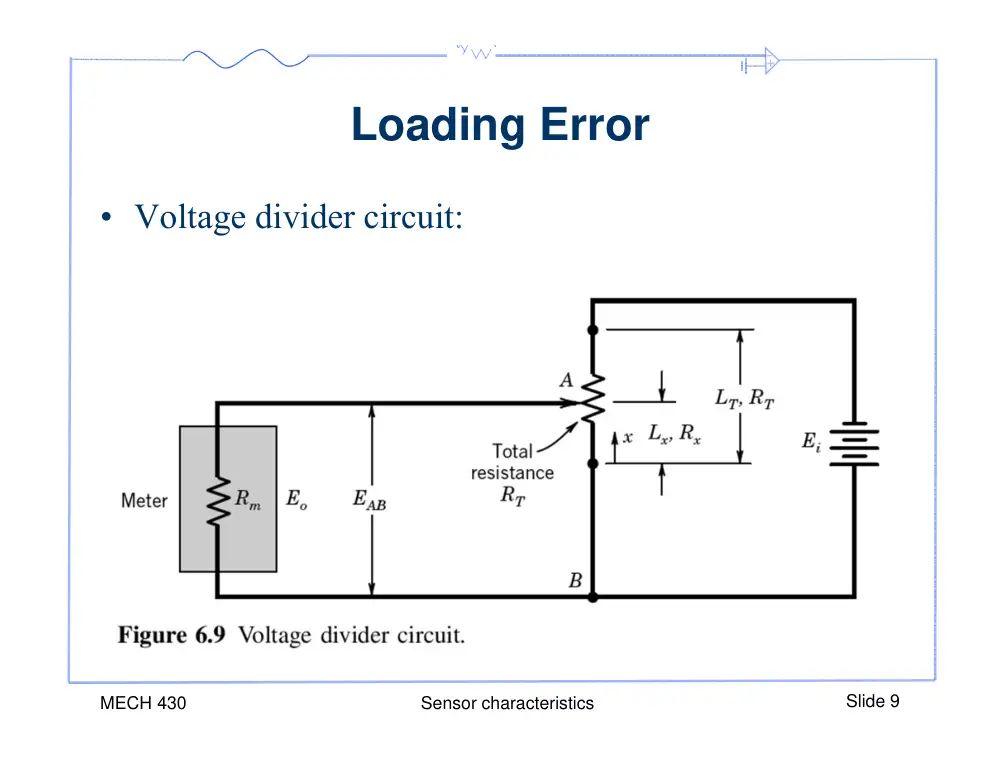
Loading Error
• Voltage divider circuit:
MECH 430
Sensor characteristics
Slide 9
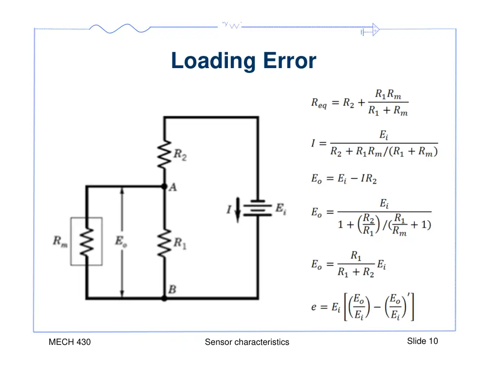
Loading Error
MECH 430
Sensor characteristics
Slide 10
6.4 Bridge Circuits
• Bridge circuits have been devised for measurement of
capacitance, inductance and most often for Resistance
measurement.
• Resistive bridge is called Wheatstone Bridge provides
means for accurately measuring resistance, and
detecting small resistance changes.
MECH 430
Introduction
Slide 11
MECH 430
SC_Bridge_circuits
Slide 12
Resistive Bridge Circuit
• Resistive bridge circuits are used in measurement of
temperature, pressure, strain, force, magnetic fields…
• One or more legs may be a thermistor, strain gauge,
RTD, piezoresistive element, potentiometer, …
• The input excitation VR can be ac or dc.
MECH 430
SC_Bridge_circuits
Slide 13
The balanced condition
• If Rm>> all R’s, the bridge acts like an open circuit
and im = 0.
3
2
2
4
1
1
R
R
V
i
R
R
V
i
R
R
R
CB
R
AB
R V
R
R
i R
V
R V
R
R
i R
V
3
2
2
2
2
4
1
1
1
1
CB
AB
BC
AB
AC
o
V
V
V
V
V
V
(1)
(2)
(3)
(4)
(5)
Vo
MECH 430
SC_Bridge_circuits
Slide 14
The balanced condition
• Subbing (3) & (4) into (5) gives:
R
o
R V
R
R
R
R R
R R
V
3
2
4
1
4
2
1 3
If Vo = 0 then R1R3 = R2R4
k
R
R
R
R
3
2
4
1
(6)
(7)
Condition for a balanced bridge
MECH 430
SC_Bridge_circuits
Slide 15
Operating modes of bridge circuits
• Bridges may be operated in deflection (unbalanced)
mode, or null-balanced mode.
Vo
R2
R3
Rx
R4
VR
B
D
A
C
MECH 430
SC_Bridge_circuits
Slide 16
The unbalanced mode
• Starting from a balanced state, if the sensor resistance
Rx changes by x, a voltage across the bridge diagonal is
generated (i.e., V0 ≠ 0).
• Vo can be used to compute this change using a
calibrated meter.
• Vo is a nonlinear function of unbalance x. This method
is suitable for small changes in resistors (x < 0.005).
The unbalanced mode
MECH 430
Introduction
Slide 17
R
o
R V
R
R
R
R R
R R
V
3
2
4
1
4
2
1 3
MECH 430
SC_Bridge_circuits
Slide 18
The null-balanced mode
• This mode requires that the bridge is always maintained at a
balanced state (i.e., Vo = 0).
• To satisfy this condition, we have to vary one of resistor
(e.g., R2) by a control circuit based on the change in Rx.
• Any change in Rx causes a meter deflection and an error
signal is generated by a control circuit which modifies R2
until its effect cancels that of Rx and the bridge is balanced
again.
• The advantages of this method is that the input voltage need
not be known, and current detector is needed instead of a
current sensor.
Example 6.3
• A Temp sensor changes it resistance with temp according to:
– R is current sensor resistance
– R0 is sensor resistance at T0
– T is current temperature
– T0 is temperature reference at 0ºC
– Alpha is constant = 0.00395ºC-1
• It is connected to a deflection bridge at the R1 location where
initially all arms are equal to 100Ω. The supply voltage is 10V.
• If the temperature of R1 is changed so that Vo is equal to
0.569V, What is the temp of the sensor?
MECH 430
Introduction
Slide 19
MECH 430
SC_amplification
Slide 20
6.6 Signal Amplification
•
The simplest form of signal processing is signal
amplification.
•
The need arises because transducers provide signal
that are said `weak’ (i.e, μV or mV), and are too small
for reliable processing.
•
Standard electronics data processors (A/D, frequency
modulators) require signals of sizeable amount (Volts
and mA).
MECH 430
SC_amplification
Slide 21
6.6 Signal Amplification
•
Usually the raw signal is multiplied by a constant:
–
Voltage gain AV up to 1000,
–
Current gain AI up to 106.
•
Amplification maximizes the use of available voltage
range to:
–
Increase accuracy,
–
Increase Signal to Noise Ratio (SNR).
MECH 430
SC_amplification
Slide 22
Linearity & Distortion
•
Linearity in amplifiers is important, such that when
we feed a signal to an amplifier, we want the output
signal of the amplifier to be an exact replica of the
input, except of course for having a larger amplitude.
•
Any change in waveform is considered to be a
distortion, and is undesirable.
MECH 430
SC_amplification
Slide 23
Linearity & distortion
•
An amplifier that preserves the relationship between
input and output is called a linear amplifier and is
characterized by:
( )
( )
Av t
t
v
i
o
•
If this relationship contains higher powers of vi then
the amplifier is said to exhibit nonlinear distortion.
Amplifier gain
MECH 430
SC_amplification
Slide 24
Signal Amplification
• The amplification discussed so far operate on small
input signals and are known as voltage amplifiers (will
be used here).
• Another type of amplifier is the power amplifier that
provides a modest amount of voltage gain but
substantial current gain.
• Power amplifiers absorb little power from the input but
deliver large amounts of power to its load.
MECH 430
SC_amplification
Slide 25
The raw signal generated by
most passive sensors may be
in the order of mV or nA.
A thermocouple with one iron arm
(high emf at +3.54mV) and one
nickel arm (low emf at – 3.1mV)
produces an output of 6.64 mV for
∆T =200oC.
A photodiode has a current
output of 10μA when illuminated
and 10nA in total darkness.
Typical signal range of common sensors
CF is added
to provide
noise filtering.
CF
RF
i
i
F
out
iR
V
Sensing
junction
Material 2
Material 1 Reference
MECH 430
SC_amplification
Slide 26
Operational Amplifier (Op-amp)
•
The first types of op-amps were constructed from
vacuum tubes and then transistors and resistors, but
built separately.
•
The first Integrated Circuit (IC) op-amp was
manufactured in the 1960. In this chip, all resistors and
transistors were integrated onto a single silicon chip.
•
A nice feature about op-amps is that they operate at
levels close to their predicted theoretical performance.
•
Op-amps will be studied in this course as a black boxes
(i.e., we will not study their internals), where we will
study how they are used in circuits.
OP-AMP Applications
MECH 430
Introduction
Slide 27
Operational Amplifier
MECH 430
Introduction
Slide 28
Operational Amplifier
MECH 430
Introduction
Slide 29
MECH 430
SC_amplification
Slide 30
Op-Amp Terminals
•
An op-amp has 5 terminals:
–
3 terminal for signal flow: 2 inputs(1,2) and 1 output (3),
–
2 terminals for power (4,5).
•
In addition to these terminals an op-amp can have
other terminals for specific purposes (e.g., offset
nulling, not covered here).
MECH 430
SC_amplification
Slide 31
Ideal Op-amp
•
An ideal op-amp senses the difference between the
voltage (with respect to ground) of signals applied at
its two terminals (v2-v1) multiplies it by a number A
and causes a resulting voltage A(v2-v1) at terminal 3.
1
2
3
+
-
+
v1
v2
+-
+-
+-
1
2
v
A v
Power supply
1 0
i
i2 0
MECH 430
SC_amplification
Slide 32
Ideal Op-amp
•
At its inputs:
–
Draws zero current at its inputs,
–
The input impedance is infinite.
•
At its output:
–
Acts as an ideal voltage source.
–
This means that regardless of how much current the
output load is drawing, the op-amp and keep up and
the voltage at the output does not drop.
–
The output impedance is zero.
1
2
3
+
-
+
v1
v2
+-
+-
+-
1
2
v
A v
Power supply
1 0
i
i2 0
MECH 430
SC_amplification
Slide 33
Ideal Op-amp
•
The output voltage is in phase (has the same sign)
as the v2 but opposite sign than v1.
•
For this reason v1 is called the inverting terminal
and v2 is called the non-inverting terminal.
1
2
3
+
-
+
v1
v2
+-
+-
+-
1
2
v
A v
Power supply
1 0
i
i2 0
MECH 430
SC_amplification
Slide 34
Common mode
rejection
•
Note that the op-amp amplifies the difference
between the two terminals. Therefore if both
terminals are corrupted by similar noise, this noise
will not be amplified (beauty of an op-amp).
•
This property is called common mode rejection.
•
Note that the gain A is called differential gain
(usually of the order of 105 to 106).
1
2
3
+
-
+
v1
v2
+-
+-
+-
1
2
v
A v
Power supply
2 0
i
i1 0
MECH 430
SC_amplification
Slide 35
Ideal Op-amp
1
2
3
+
-
+
v1
v2
+-
+-
+-
1
2
v
A v
Power supply
1 0
i
2 0
i
CC
n
p
CC
CC
n
p
CC
n
p
CC
n
p
CC
o
V
v )
A(v
V
V
v )
A( v
V
v )
A(v
V
v )
A( v
V
v
MECH 430
SC_amplification
Slide 36
Ideal Op-amp
•
Given that the feedforward open loop gain (i.e.,
from input to output without any looping back) is
very large, they are rarely used in open loop.
•
Rather, op-amps are usually used in feedback,
closing the loop around the op-amp.
1
2
3
+
-
+
v1
v2
+-
+-
+-
1
2
v
A v
Power supply
1 0
i
i2 0
Ideal Op-Amp
• In the linear region of operation of the op-amp:
• This golden rule is not valid if the op-amp is operating in the
saturated region.
• To operate in the linear region, a negative feedback from the
output to the inverting input of the op-amp must be present.
• If a circuit containing an op amp does not provide a negative
feedback path from the op-amp output to the inverting input,
then the op-amp will normally saturate
• Finally, note that, even with negative feedback, operation in
the linear region is not guaranteed!
MECH 430
Introduction
Slide 37
n
p
v v
MECH 430
SC_amplification
Slide 38
Inverting op-amps
•
We get an inverting amplifier by:
1)
Connecting a resistor in the negative feedback,
2)
Connecting a resistor between the voltage source and
the op amp negative terminal,
3)
Connecting the non-inverted terminal to ground.
MECH 430
SC_amplification
Slide 39
Closed-loop gain
•
In this case: v2 ≈ v1.
•
In such systems we say the two terminals are
``tracking each other in potential’’.
•
We also speak of a virtual short circuit between
the two terminals.
•
We speak of terminal 1 as being a virtual ground.
0
)
(
1
2
1
2
A
v
v
v
v
A v
v
o
o
1i
MECH 430
SC_amplification
Slide 40
Closed-loop gain
•
The current through R1 is:
1
1
1
1
R
v
R
v
v
i
i
i
•
The voltage across R2 is:
2
1
0
R R
v
v
i
o
1
2
R
R
v
v
i
o
•
The closed loop gain is:
MECH 430
SC_amplification
Slide 41
Closed-loop gain
•
This is a very interesting results and states that we
can make the gain of the op-amp as accurate as we
want by selecting passive components (i.e.,
resistors) of appropriate accuracy.
•
It also means that the closed loop gain of the op-
amp is independent of the op amp internal gain.
1
2
R
R
v
v
i
o
1i
MECH 430
SC_amplification
Slide 42
Equivalent circuit
• The input resistance of the equivalent circuit is found as:
+
-
iv
R
R
1
2
iv
o 0
R
+
-
R1
Ri
1
1
1
R
R
v
v
i
v
R
i
i
i
in
• The inverting configuration suffers from a low input
resistance.
MECH 430
SC_amplification
Slide 43
Other applications of inverting op-
amps
•
If we replace the resistances by impedances:
1
2
Z
Z
V
V
i
o
MECH 430
SC_amplification
Slide 44
Miller Integrator
•
For instance if we use a resistor and capacitor, the
resulting circuit acts as an integrator:
jwCR
sCR
V
V
i
o
1
1
R
v t
i
i
)
(
1
vo(t) VC
i1(t)
0
t
C
vo(t) VC 1
CR
vi(t)
0
t
In Laplace:
MECH 430
SC_amplification
Slide 45
Miller Integrator
•
This circuit is known as the Miller integrator.
•
At zero frequency (dc) the gain is infinite and the
circuit operates as open loop.
vo(t) VC 1
CR
vi(t)
0
t
Initial voltage across
capacitor
Integration time
constant
MECH 430
SC_amplification
Slide 46
Differentiator
•
If we use the capacitor for Z1 and the resistor for Z2
the circuit acts as a differentiator:
jwCR
sCR
V
V
i
o
dt
CR dv t
t
v
i
o
( )
( )
MECH 430
SC_amplification
Slide 47
Differentiator
• The differentiator circuit is a noise amplifier.
• A spike is introduced every time there is a sharp change
in vi(t). Such a spike could be picked-up interference.
• For this reason differentiator circuits are usually avoided
in practice.
MECH 430
SC_amplification
Slide 48
Weighted Summer
•
Another application of an inverting op-amp:
3
3
3
2
2
2
1
1
1
,
,
R
v
i
R
v
i
R
v
i
f
o
iR
v
3
3
2
2
1 1
v
R
R
v
R
R
v
R
R
v
f
f
f
o
MECH 430
SC_amplification
Slide 49
Weighted summer, opposite signs
•
To include opposite signs use 2 op-amps:
vo v1
Ra
R1
Rc
Rb
v2
Ra
R2
Rc
Rb
v2
Rc
R3
v4
Rc
R4
MECH 430
SC_amplification
Slide 50
Non-inverting op-amp
•
In a non-inverting op-amp the input signal is applied
to the positive terminal, while the negative terminal is
connected to ground.
1
1
R
v
i
i
0
1
2
A
v
v
v
o
1
2
2
1
1
R
R
v
v
R
R
v
v
v
i
o
i
i
o
MECH 430
SC_amplification
Slide 51
Non-inverting amplifier
•
The property of infinite input impedance enables
using the circuit as a buffer amplifier, where a source
with high impedance connects to a load with low
impedance.
•
The buffer amplifier is used as an impedance
transformer.
+
-
iv
R
R
1
2
1
iv
o 0
R
+
-
iR
MECH 430
SC_amplification
Slide 52
Buffer op-amp
•
The buffer amplifier can also be constructed by
making R2 = 0 and R1 = ∞.
•
This circuit is referred to as a voltage follower, since
the output follows the input.
MECH 430
SC_amplification
Slide 53
Difference Amplifier
•
We need to find the expression of the output voltage
vo in terms of the input voltages v1 and v2.
Difference Amplifier
MECH 430
Introduction
Slide 54
Difference Amplifier
MECH 430
Introduction
Slide 55
MECH 430
SC_amplification
Slide 56
Problem with a difference amplifier
• Looking at the difference voltage supply
• The resistance seen by vId is called the differential input
resistance RId
• A drawback of a difference amplifier is that RId is finite
RId vId
i1
vId R1i1 0 R1ii
RId 2R1
Loop equation:
MECH 430
SC_amplification
Slide 57
Instrumentation amplifier
•
A much better type of instrumentation amplifier is shown below.
•
The circuit consists of two stages:
–
Stage 1: Two op-amps with three resistors,
–
Stage 2: One difference amplifier.
Instrumentation amplifier
MECH 430
Introduction
Slide 58
MECH 430
SC_amplification
Slide 59
Instrumentation amplifier
•
The virtual short circuits at the inputs of op-amps A1
and A2 cause the voltages v1 and v2 to appear at the two
terminals of the resistor R1.
•
A current i = (v1-v2)/2R1 flows through 2R1 and the two
resistors R2.
MECH 430
SC_amplification
Slide 60
Instrumentation amplifier
•
Any common-mode signal vCM results in NO current
flowing through R1 and therefore vo1= vo2= 0.
•
The second stage amplifier senses No voltage gradient
and produces zero output voltage.
Amplification
Difference