
EECE 320 Lecture 18, Fall 2011
American University of Beirut · Digital Systems Design · 9 pages · Prof. Ali Chehab
More EECE 320 files
Show the text of this lab
EECE 320 L18: Combinational Logic design Practices 1
Chehab, AUB, 2003
EECE 320
Digital Systems Design
Lecture 18:
Sequential Logic Design
Principles
Ali Chehab
EECE 320 L18: Combinational Logic design Practices 2
Chehab, AUB, 2003
Introduction
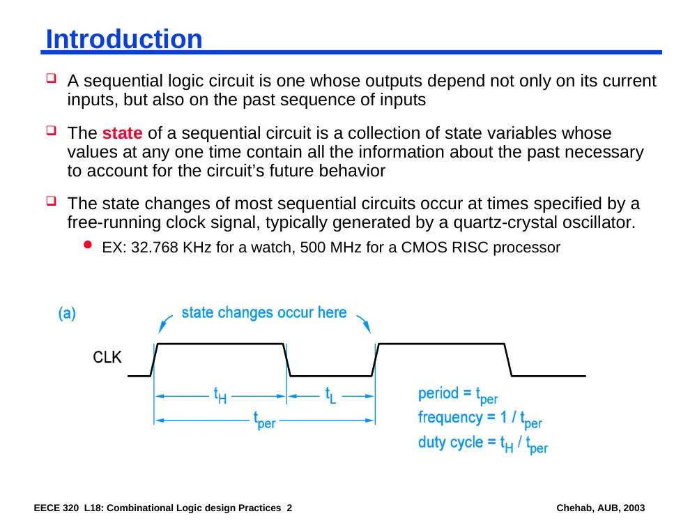
A sequential logic circuit is one whose outputs depend not only on its current
inputs, but also on the past sequence of inputs
The state of a sequential circuit is a collection of state variables whose
values at any one time contain all the information about the past necessary
to account for the circuit’s future behavior
The state changes of most sequential circuits occur at times specified by a
free-running clock signal, typically generated by a quartz-crystal oscillator.
EX: 32.768 KHz for a watch, 500 MHz for a CMOS RISC processor
EECE 320 L18: Combinational Logic design Practices 3
Chehab, AUB, 2003
Bistable Elements – Digital Analysis
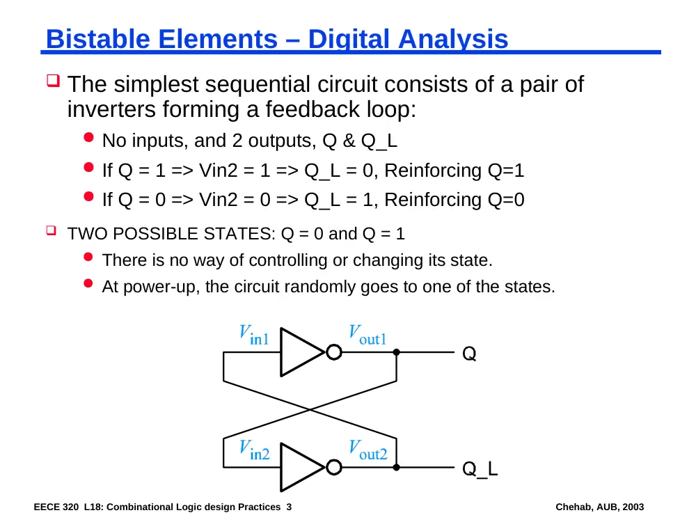
The simplest sequential circuit consists of a pair of
inverters forming a feedback loop:
No inputs, and 2 outputs, Q & Q_L
If Q = 1 => Vin2 = 1 => Q_L = 0, Reinforcing Q=1
If Q = 0 => Vin2 = 0 => Q_L = 1, Reinforcing Q=0
TWO POSSIBLE STATES: Q = 0 and Q = 1
There is no way of controlling or changing its state.
At power-up, the circuit randomly goes to one of the states.
EECE 320 L18: Combinational Logic design Practices 4
Chehab, AUB, 2003
Bistable Elements – Analog Analysis
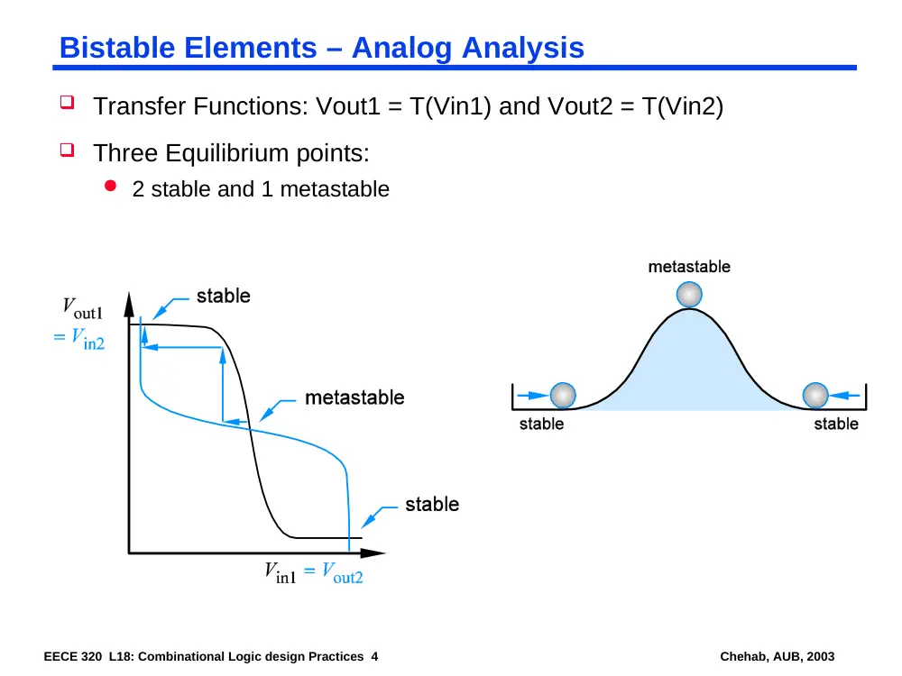
Transfer Functions: Vout1 = T(Vin1) and Vout2 = T(Vin2)
Three Equilibrium points:
2 stable and 1 metastable
EECE 320 L18: Combinational Logic design Practices 5
Chehab, AUB, 2003
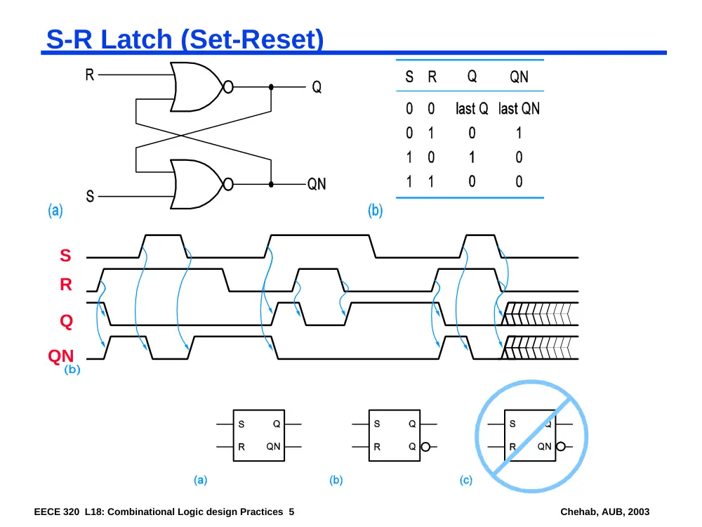
S-R Latch (Set-Reset)
S
R
Q
QN
EECE 320 L18: Combinational Logic design Practices 6
Chehab, AUB, 2003
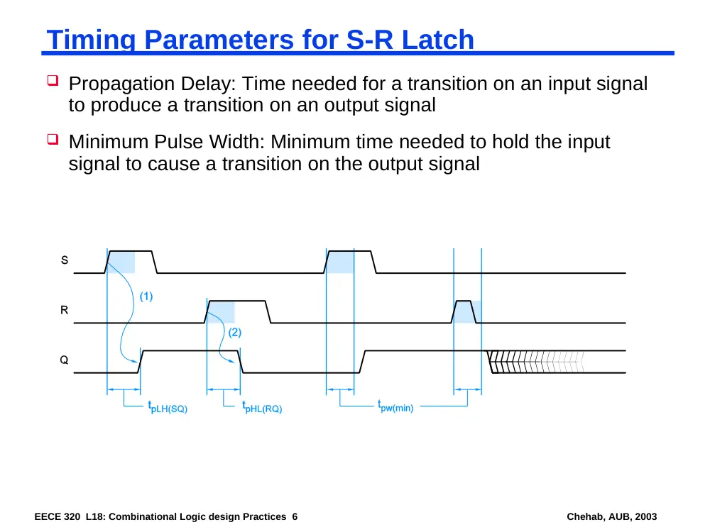
Timing Parameters for S-R Latch
Propagation Delay: Time needed for a transition on an input signal
to produce a transition on an output signal
Minimum Pulse Width: Minimum time needed to hold the input
signal to cause a transition on the output signal
EECE 320 L18: Combinational Logic design Practices 7
Chehab, AUB, 2003
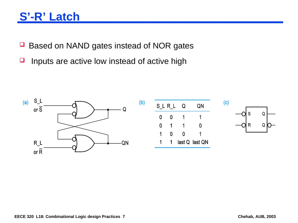
S’-R’ Latch
Based on NAND gates instead of NOR gates
Inputs are active low instead of active high
EECE 320 L18: Combinational Logic design Practices 8
Chehab, AUB, 2003
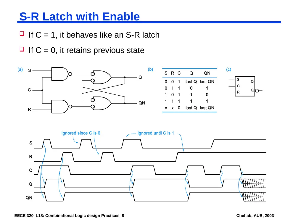
S-R Latch with Enable
If C = 1, it behaves like an S-R latch
If C = 0, it retains previous state
EECE 320 L18: Combinational Logic design Practices 9
Chehab, AUB, 2003
Next Lecture and Reminders
Next lecture
Reminders