
EECE 320 Lecture 29, Fall 2011
American University of Beirut · Digital Systems Design · 26 pages · Prof. Ali Chehab

Showing the first 10 of 26 pages. Download the PDF to see all of it.
More EECE 320 files
Show the text of this lab
EECE 320 L29: Sequential Logic design Practices 1
Chehab, AUB, 2003
EECE 320
Digital Systems Design
Lecture 29:
Sequential Logic Design
Practices
Ali Chehab
EECE 320 L29: Sequential Logic design Practices 2
Chehab, AUB, 2003
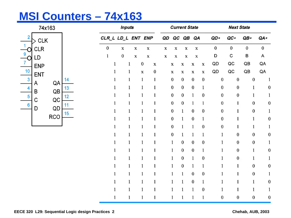
MSI Counters – 74x163
EECE 320 L29: Sequential Logic design Practices 3
Chehab, AUB, 2003
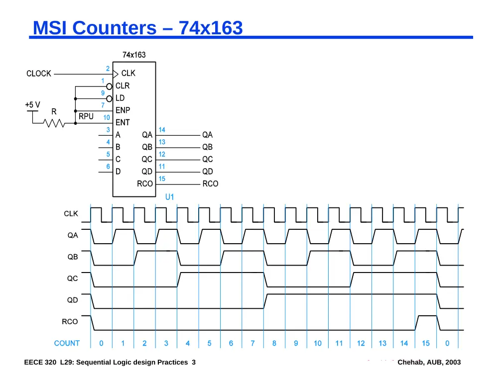
MSI Counters – 74x163
EECE 320 L29: Sequential Logic design Practices 4
Chehab, AUB, 2003
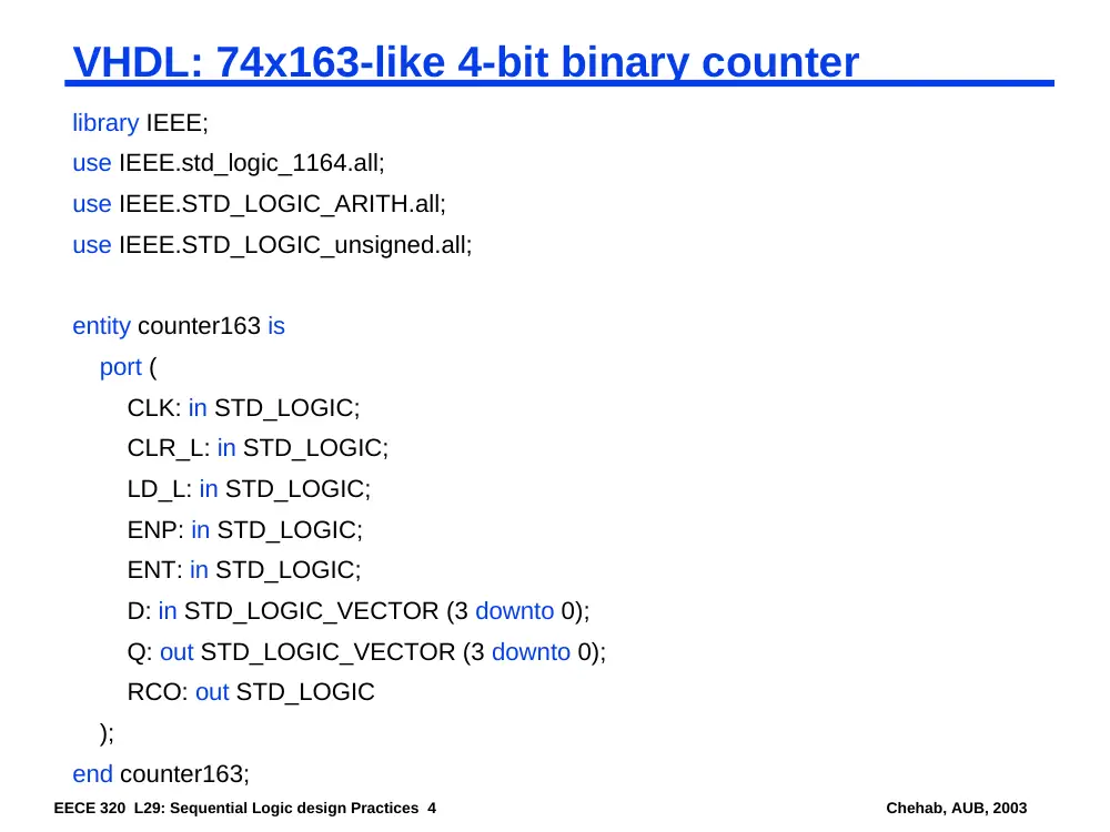
VHDL: 74x163-like 4-bit binary counter
library IEEE;
use IEEE.std_logic_1164.all;
use IEEE.STD_LOGIC_ARITH.all;
use IEEE.STD_LOGIC_unsigned.all;
entity counter163 is
port (
CLK: in STD_LOGIC;
CLR_L: in STD_LOGIC;
LD_L: in STD_LOGIC;
ENP: in STD_LOGIC;
ENT: in STD_LOGIC;
D: in STD_LOGIC_VECTOR (3 downto 0);
Q: out STD_LOGIC_VECTOR (3 downto 0);
RCO: out STD_LOGIC
);
end counter163;
EECE 320 L29: Sequential Logic design Practices 5
Chehab, AUB, 2003
VHDL: 74x163-like 4-bit binary counter
architecture counter163 of counter163 is
signal IQ: std_logic_vector(3 downto 0):= (others => '0');
begin
process (CLK, ENT, IQ)
begin
if (CLK'event and CLK = '1') then
if CLR_L = '0' then IQ <= (others => '0');
elsif LD_L = '0' then IQ <= D;
elsif (ENT and ENP) = '1' then IQ <= IQ + 1;
end if;
end if;
if (IQ = 15) and (ENT = '1') then RCO <= '1';
else RCO <= '0';
end if;
Q <= IQ;
end process;
end counter163;
EECE 320 L29: Sequential Logic design Practices 6
Chehab, AUB, 2003
Shift Registers
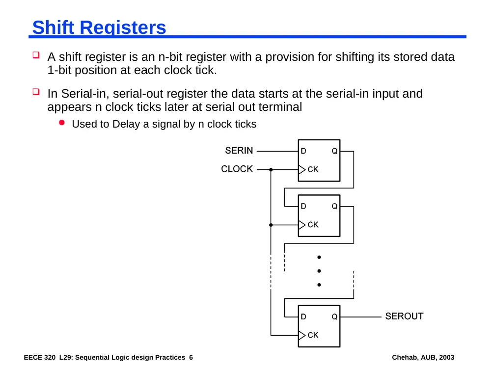
A shift register is an n-bit register with a provision for shifting its stored data
1-bit position at each clock tick.
In Serial-in, serial-out register the data starts at the serial-in input and
appears n clock ticks later at serial out terminal
Used to Delay a signal by n clock ticks
EECE 320 L29: Sequential Logic design Practices 7
Chehab, AUB, 2003
Shift Registers
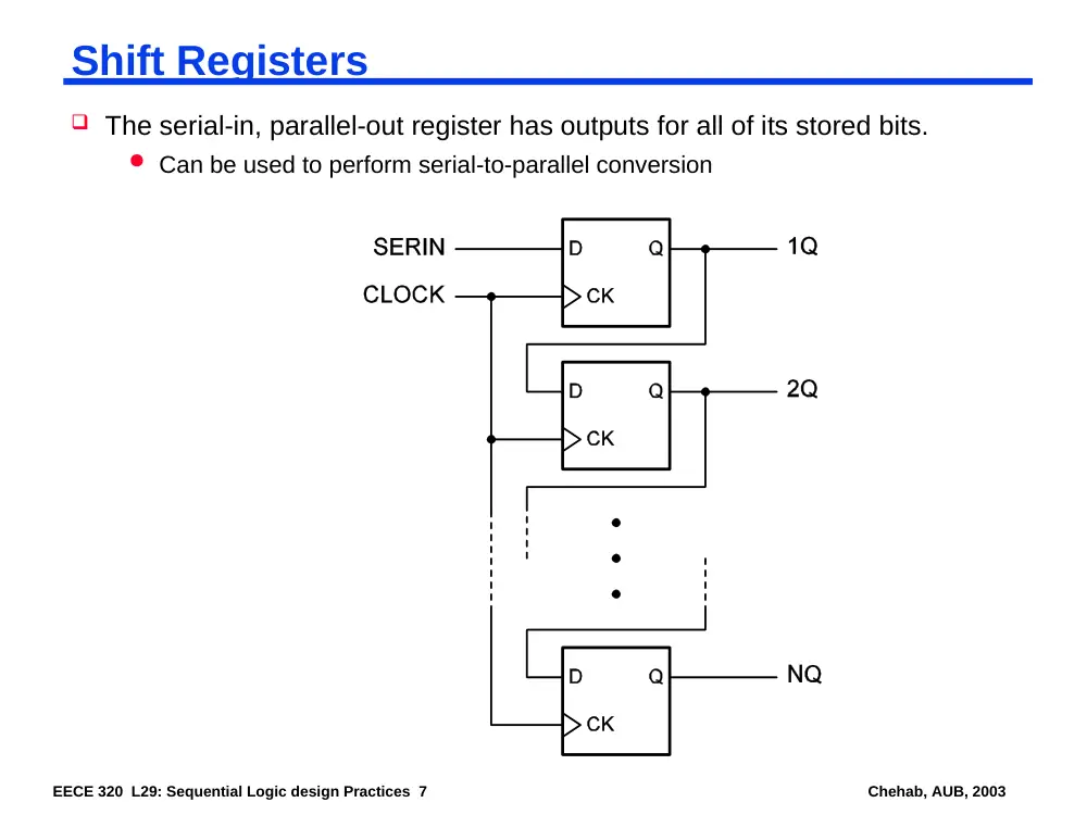
The serial-in, parallel-out register has outputs for all of its stored bits.
Can be used to perform serial-to-parallel conversion
EECE 320 L29: Sequential Logic design Practices 8
Chehab, AUB, 2003
Shift Registers
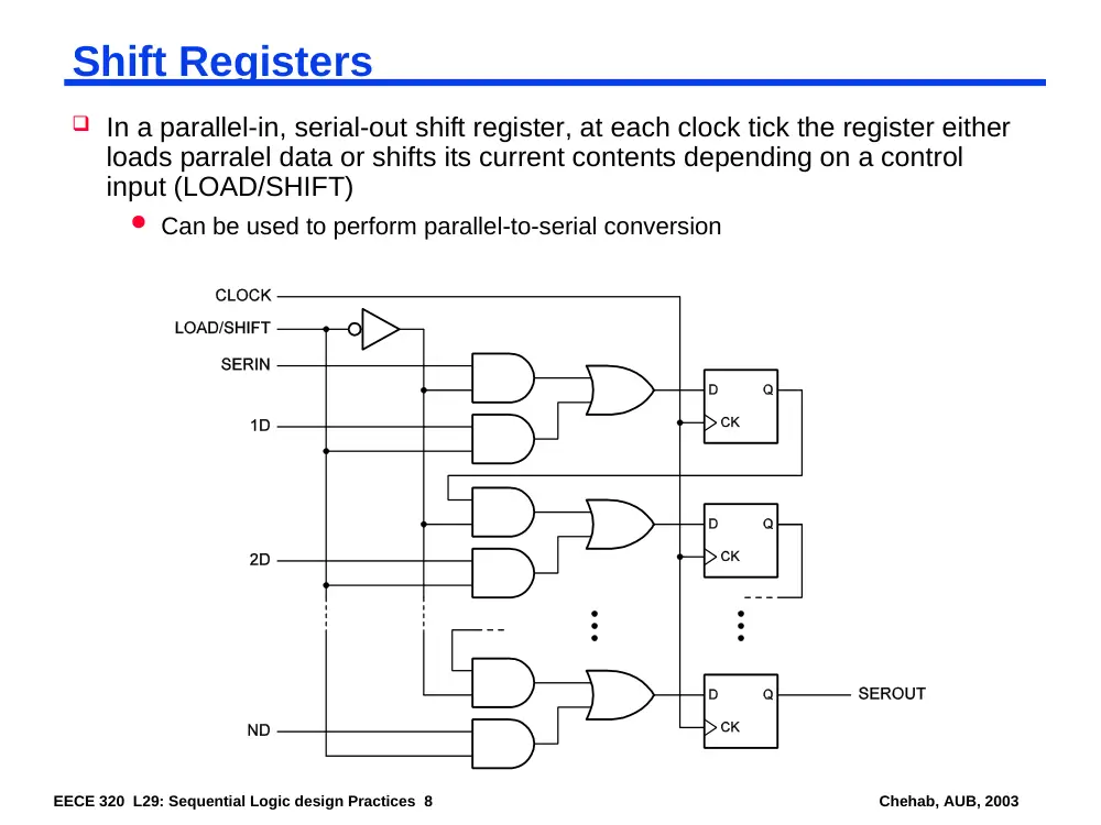
In a parallel-in, serial-out shift register, at each clock tick the register either
loads parralel data or shifts its current contents depending on a control
input (LOAD/SHIFT)
Can be used to perform parallel-to-serial conversion
EECE 320 L29: Sequential Logic design Practices 9
Chehab, AUB, 2003
Shift Registers
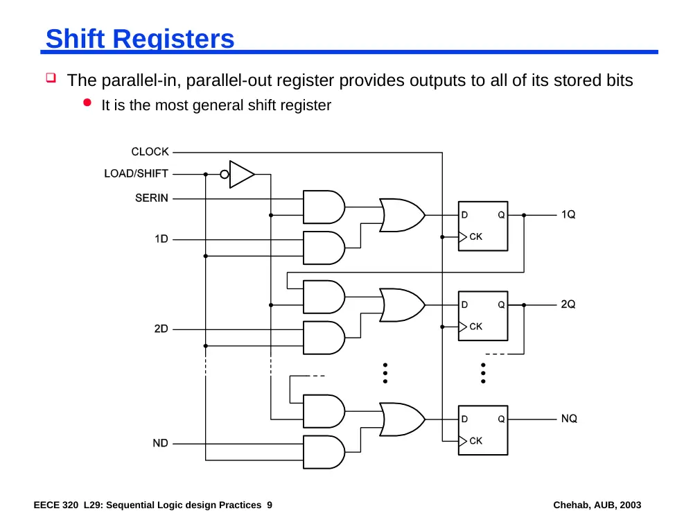
The parallel-in, parallel-out register provides outputs to all of its stored bits
It is the most general shift register
EECE 320 L29: Sequential Logic design Practices 10
Chehab, AUB, 2003
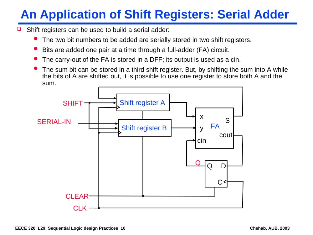
An Application of Shift Registers: Serial Adder
Shift registers can be used to build a serial adder:
The two bit numbers to be added are serially stored in two shift registers.
Bits are added one pair at a time through a full-adder (FA) circuit.
The carry-out of the FA is stored in a DFF; its output is used as a cin.
The sum bit can be stored in a third shift register. But, by shifting the sum into A while
the bits of A are shifted out, it is possible to use one register to store both A and the
sum.
SERIAL-IN
D
C
Q
Shift register A
CLK
SHIFT
FA
x
y
cin
S
cout
Shift register B
CLEAR
Q
EECE 320 L29: Sequential Logic design Practices 11
Chehab, AUB, 2003
Operation of the Serial Adder
Initially, both shift registers and the DFF (carry) are cleared.
The first number to be added is shifted into B.
The contents of B are shifted out through the FA and the sum is stored in A. This operation
is equivalent to copying B into A since A was initially zero.
While B is shifted through the FA, a second number is transferred to it through its serial
input.
At any clock cycle, shift registers A and B provide two bits to the FA, while the output of the
DFF provides the carry in.
The shift control enables both registers and the DFF , so at the next clock pulse, both
registers are shifted once to the right, the sum bit enters the leftmost flip-flop of A, and the
output carry is transferred into the DFF.
The shift control enables the registers for a number of clock pulses equal to the number of
bits in the registers.
For each succeeding clock pulse, a new sum bit is transferred to A, a new carry is
transferred to Q, and both registers are shifted once to the right.
The process repeats until the shift control is disabled.
EECE 320 L29: Sequential Logic design Practices 12
Chehab, AUB, 2003
Universal Shift Register
A universal shift (bidirectrional) register has the following capabilities:
Asynchronous clear
Shift-right control
Shift-left control
Parallel load
N parallel output lines
A control state that leaves the information in the register unchanged in the
presence of the clock
Function table:
Mode control
S1
S0
Register Operation
0
0
No change
0
1
Shift right
1
0
Shift left
1
1
Parallel load
EECE 320 L29: Sequential Logic design Practices 13
Chehab, AUB, 2003
Universal Shift Register
CLK
A3
I3
CLEAR
D
C
Q
3 2
1 0
A2
D
C
Q
3 2
1 0
A1
D
C
Q
3 2
1 0
A0
D
C
Q
3 2
1 0
SH-IN for
Shift right
S1
S0
I2
I1
I0
SH-IN for
Shift left
EECE 320 L29: Sequential Logic design Practices 14
Chehab, AUB, 2003
MSI Shift Registers
CLK
CLR
SERA
SERB
QA
QB
QC
QD
QE
QF
QG
QH
74x164
74x164
8-bit shift register
Serial-in Parallel-out
Asynchronous Clear
SERA, SERB are ANDed together
EECE 320 L29: Sequential Logic design Practices 15
Chehab, AUB, 2003
MSI Shift Registers
74x166
8-bit shift register
Parallel-in Serial-out
Asynchronous Clear
CLK and CLKINH are NORed together. When CLKINH = 1 HOLD mode
CLK
CLKINH
SH/LD
CLR
SER
A
B
C
D
E
F
G QH
H
EECE 320 L29: Sequential Logic design Practices 16
Chehab, AUB, 2003
MSI Shift Registers
74x194
4-bit Bidirectional (shifted in 2 directions), parallel-in, parallel-out
Data can be held, loaded, shifted left or right based on the values of S1
and S0
CLK
CLR
S1
S0
LIN
D QD
C QC
B QB
A QA
RIN
EECE 320 L29: Sequential Logic design Practices 17
Chehab, AUB, 2003
VHDL: 8-bit PIPO General Shift Register
library IEEE;
use IEEE.std_logic_1164.all;
entity Vshiftreg is
port (
CLK, CLR, RIN, LIN: in STD_LOGIC;
S: in STD_LOGIC_VECTOR (2 downto 0);
D: in STD_LOGIC_VECTOR (7 downto 0);
Q: out STD_LOGIC_VECTOR (7 downto 0)
);
end Vshiftreg ;
EECE 320 L29: Sequential Logic design Practices 18
Chehab, AUB, 2003
VHDL: 8-bit PIPO General Shift Register
architecture Vshiftreg of Vshiftreg is
signal IQ: std_logic_vector(7 downto 0);
begin
process (CLK, CLR, IQ)
begin
if CLR = ‘1' then IQ <= (others => '0');
elsif (CLK'event and CLK = '1') then
case CONV_INTEGER(S) is
when 0 => null;
when 1 => IQ <= D;
when 2 => IQ <= RIN & IQ(7 downto 1);
when 3 => IQ <= IQ(6 downto 0) & LIN;
when 4 => IQ <= IQ(0) & IQ(7 downto 1);
when 5 => IQ <= IQ(6 downto 0) & IQ(7);
When 6 => IQ <= IQ(7) & IQ(7 downto 1);
when 7 => IQ <= IQ(6 downto 0) & ‘0’;
when others => null;
end case;
end if;
Q <= IQ;
end process;
end Vshiftreg;
EECE 320 L29: Sequential Logic design Practices 19
Chehab, AUB, 2003
Shift Register Counters
A shift register can be combined
with combinational logic to form a
state machine whose state
diagram is cyclic
Ring counter: It uses an n-bit shift
register to obtain a counter with n
states
Example: 74x194
When RESET is active, it loads
0001
When RESET is low, it performs
left shift
Next states: 0010, 0100, 1000,
0001, …
It is not robust, if it gets off the
normal cycle it stays off it.
EECE 320 L29: Sequential Logic design Practices 20
Chehab, AUB, 2003
Shift Register Counters
EECE 320 L29: Sequential Logic design Practices 21
Chehab, AUB, 2003
Ring Counter State Diagram
EECE 320 L29: Sequential Logic design Practices 22
Chehab, AUB, 2003
Self-Correcting Counter
It is designed so that all abnormal states have transitions leading to normal
states in analogy with minimum-risk approach of an FSM
EECE 320 L29: Sequential Logic design Practices 23
Chehab, AUB, 2003
Self-Correcting Counter
EECE 320 L29: Sequential Logic design Practices 24
Chehab, AUB, 2003
Johnson Counter
The complement of the serial output is fed back into the serial input
It has 2n states
EECE 320 L29: Sequential Logic design Practices 25
Chehab, AUB, 2003
Johnson Counter
EECE 320 L29: Sequential Logic design Practices 26
Chehab, AUB, 2003
Next Lecture and Reminders
Next lecture
Reminders