
MECH 430 Problems Operational Amplifiers, Fall 2011
American University of Beirut · Instrumentation and Measurements · 9 pages



More MECH 430 files
- Problems Solutions of Operational Amplifiers Problems · Fall 2011Problems · with solutionView
- Homework 3 · Spring 2017HomeworkView
- Homework Lecture Assignment · Spring 2017LabView
- Project Pumping Station · Spring 2017ProjectView
- Final · Spring 2015Final examView
- Notes 4 · Spring 2014NotesView
- Notes 3 · Spring 2014NotesView
- Notes 7 · Spring 2014NotesView
Show the text of this problems
open-loop gain, is very large (107 to 10°) and ideally infi-
nite; and has an infinite input resistance and a zero output
resistance.
Negative feedback is applied to an op amp by connecting
a passive component between its output terminal and its
inverting (negative) input terminal. Negative feedback
causes the voltage between the two input terminals to
become very small and ideally zero. Correspondingly, a
virtual short circuit is said to exist between the two input
terminals. If the positive input terminal is connected to
ground, a virtual ground appears on the negative input
terminal.
@ The two most important assumptions in the analysis of
op-amp circuits, presuming negative feedback exists and
the op amps are ideal, are: the two input terminals of the
op amp are at the same voltage, and zero current flows
into the op-amp input terminals.
With negative feedback applied and the loop closed,
the closed-loop gain is almost entirely determined by
external components: For the inverting configuration,
V/V; = -R2/R,; and for the noninverting configura-
tion, V,/V, = 1+R,/R,.
The noninverting closed-loop configuration features a
very high input resistance. A special case is the unity-gain
follower, frequently employed as a buffer amplifier to
connect a high-resistance source to a low-resistance load.
i
For most internally compensated op amps, the open-loop
gain falls off with frequency at a rate of -20 dB/decade,
reaching unity at a frequency f, (the unity-gain band-
width). Frequency f, is also known as the gain—bandwidth
product of the op amp: f; = Ay f,, Where Ag is the de gain,
and f, is the 3-dB frequency of the open-loop gain. At any
frequency f( > f,), the op-amp gain |A| = f/f.
eR
&
PROBLEMS
For both the inverting and the noninverting closed-loop con-
figurations, the 3-dB frequency is equal to f,/(1 + R,/R)).
The maximum rate at which the op-amp output voltage
can change is called the slew rate. The slew rate, SR, is
usually specified in V/s. Op-amp slewing can result in
nonlinear distortion of output signal waveforms.
The full-power bandwidth, fy), is the maximum frequency
at which an output sinusoid with an amplitude equal to the
op-amp rated output voltage (Vj,.,) can be produced
without distortion: fj, = SR/2zxV,
omax*
The input offset voltage, Vos, is the magnitude of de volt-
age that when applied between the op amp input termi-
nals, with appropriate polarity, reduces the dc offset
voltage at the output to zero.
The effect of Vos on performance can be evaluated by
including in the analysis a de source Vs in series with the
op-amp positive input lead. For both the inverting and the
noninverting configurations, Vos results in a de offset
voltage at the output of Vog(1 + Ry/R,).
Capacitively coupling an op amp reduces the dc offset
voltage at the output considerably.
The average of the two de currents, Jy, and Ij), that flow
in the input terminals of the op amp, is called the input
bias current, Jy. In a closed-loop amplifier, /, gives rise to
a de offset voltage at the output of magnitude /,R>. This
voltage can be reduced to Jg,R, by connecting a resistance
in series with the positive input terminal equal to the total
de resistance seen by the negative input terminal. gg is the
input offset current; that is, Jog = |Z) —- po].
Connecting a large resistance in parallel with the capaci-
tor of an op-amp inverting integrator prevents op-amp sat-
uration (due to the effect of Vos and Jy).
PROBLEMS
SECTION 2.1: THE IDEAL OP AMP
2.1 What is the minimum number of pins required for a so-
called dual-op-amp IC package, one containing two op amps?
What is the number of pins required for a so-called quad-op-
amp package, one containing four op amps?
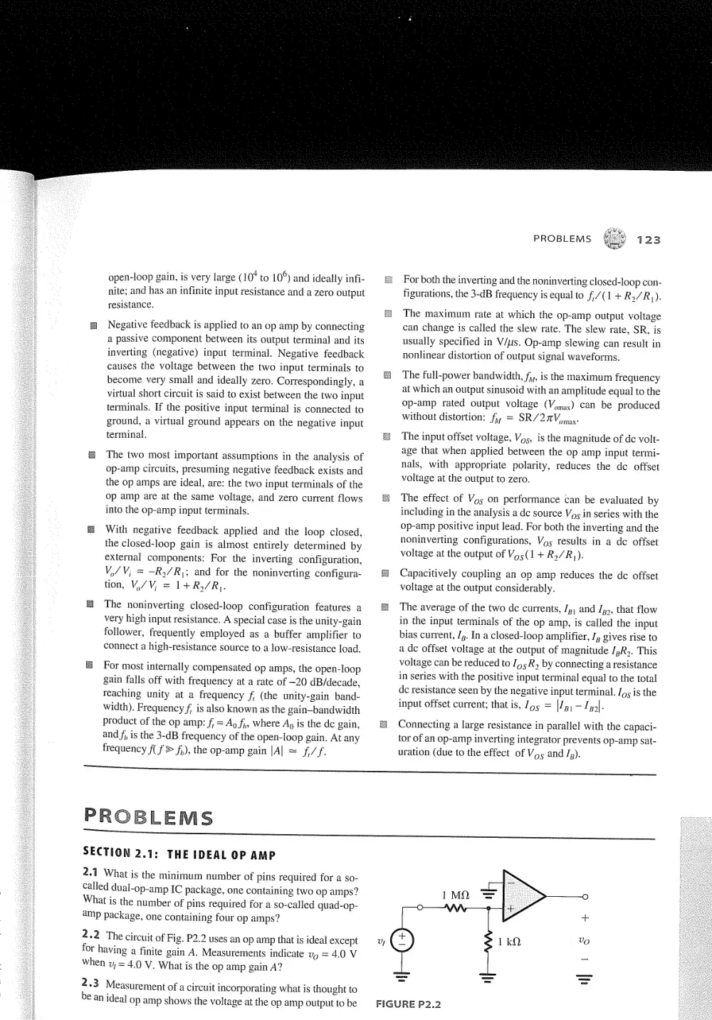
2.2 The circuit of Fig. P2.2 uses an op amp that is ideal except
for having a finite gain A. Measurements indicate vy = 4.0 V
When v, = 4.0 V. What is the op amp gain A?
2.3 Measurement of a circuit incorporating what is thought to
be an ideal op amp shows the voltage at the op amp output to be
Up
FIGURE P2.2
124 (22 CHAPTER 2 OPERATIONAL AMPLIFIERS
ative input to be -3.000 V. For the
at the
2,000 V and that atthe né
amplifier to be ideal, what would you expect the volta
d voltage at the positive input
n of the amplifier?
positive input to be? Ifthe measun
is -3.020 V, what is likely tobe the actual
2.4 A set of experiments are run on an op amp that is ideal
except for having a finite gain A. The results are tabulated
below. Are the results consistent? If not, are they reasonable,
error? What do they
in view of the possibility of experim
show the gain to be? Using this value, predict values of the mea.
surements that were accidentally omitted (the b
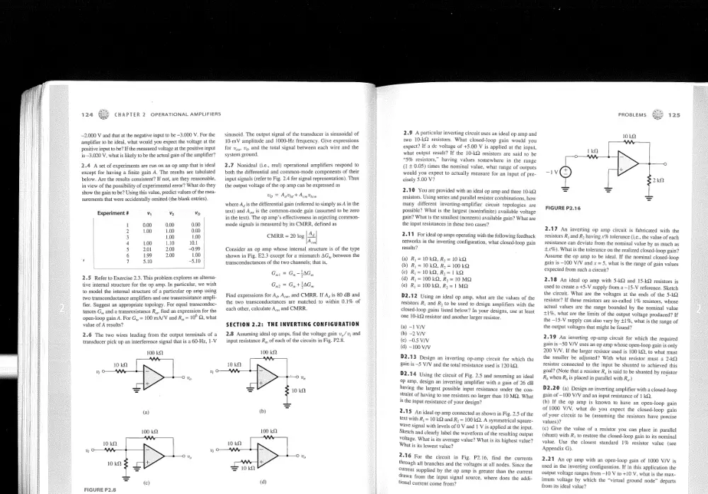
Experiment # oA ve Yo
1 000 0.00 0.00
2 10 1.00 0.00
3 1.00 1.00
4 Lio 101
5 200 © 09
6 2.00 1.00
, 7 5.10
2.5. Refer to Exercise 2.3. This problem explores an alterna-
tive internal structure for the op amp. In particular, we wish
to model the internal structure of a particular op amp using
two transconductance amplifiers and one transresistance ampli
fier. Suggest an appropriate topology. For equal transconduc:
tances G,, and a transresistance R,,, find an expression for the
100 mA/V and R,,= 10° ©, what
‘open-loop gain A. For G,
value of A results?
from the output terminals of a
ence signal that is a 60-Hz, 1-V
2.6 The two wires leadin
transducer pick up an inter
oa |
o> |
10k >
4
wid
FIGURE P2.8
sinusoid. The output signal of the transducer is sinusoidal of
10-mV amplitude and 1000-Hez frequency. Give expressions
for tay ty and the total signal between each wire and the
system ground
2.7. Nonide
both the differential and common-mode components of their
fer to Fig. 2.4 for signal representation). Thus
(ie., real) operational amplifiers respond to
input signals (r
the output voltage of the op amp can be expressed as
U9 = Ayia + Acne
where Ay the differential gain (referred to simply as A in the
text) and Ag, is the common-mode gain (assumed to be zer0
in the text), The op amp's effectiveness in rejecting common.
‘mode signals is measured by its CMRR, defined as
MRR = 20 log |4e|
ry
Consider an op amp whose internal structure is of the type
shown in Fig. E2.3 except for a mismatch AG, between the
transconductances of the two channels; that is,
Gyr = Gy 1G,
Gua = Gy + 4G,
Find expressions for Ay Age, and CMRR. If A, is 80 dB and
the two transconductances are matched to within 0.1% of
‘each other, calculate A,,, and CMRR.
SECTION 2.2: THE INVERTING CONFIGURATION
2.8. Assuming ideal op amps, find the volta
input resistance R,, of each of the circuits in Fi
100
(o)
100 k2
on
ion
NWN
Fi KO
@
icular inverting circuit uses an ideal op amp and
resistors. What closed-loop gain would you
expect? If a de voltage of +5.00 V is applied at the input,
what output result? IF the 10-kQ resistors are said to be
'5% resistors,” having values somewhere in the ran
(1+ 0.05) times the nominal value, what range of outputs
would you expect to actually measure for an input of pre-
cisely 5.00 V?
2.10 You are provided with an ideal op amp and three 10-02
resistors. Using series and parallel resistor combinations, how
many different inverting-amplifi
possible? What is the lar
circuit topologies
st (notinfinite) available voltage
gain? What is the smallest (nonzero) available gain? What are
the input resistances in these two cases?
2.11 For ideal op amps operating with the following feedback
networks in the inverting configuration, what closed-loop gain
results?
(@) Ry = 10kQ, Ry = 10k
(b) Ry = 10 kQ, R= 100 ka
(©) R= 10kQ, R= 1k
(@) R, = 100k, R, = 10 MQ
(©) R, = 100kQ, Ry =1 MQ
D2.12 Using an ideal op amp, what are the values of the
resistors Ry and R, to be used t0 design amplifiers with the
closed-loop gains listed below? In your designs, use at least
one 10-kQ resistor and another k
(a) -1viv
() 2
(©) 05 vw
(@) ~100 viv
D2.13 Design an inverting op-amp circuit for which the
fain is 5 V/V and the total resistance used is 120 Ki
02.14 Us
©p amp, desi
g the circuit of Fig. 2.5 and assuming an ideal
1 an inverting amplifier with a gain of 26 dB
having the largest possible input resistance under the con:
Strain of having to use resistors no larger than 10 MQ. What,
is the input resistance of your design?
2.15 An ideal op amp connected as shown in
text with Ry = 10k and Ry= 100 kQ. A symmetrical square-
Wave signal with levels of 0 V and 1 V is applied atthe input
Sketch and clearly label the waveform of the resulting output
Voltage. What is its average value? What is its highest value?
What is its lowest value?
2.16 For the circuit in
thro
g. P2.16, find the currents
ah all branches and the voltages at all nodes. S
current supplied by the op amp is greater than the current
4rawn from the input signal source, where does the addi
tional current come from?
PROBLEMS 125
10K
FIGURE P2.16
2.17 An inverting op amp circuit is fabricated with the
resistors Rj and R having x% tolerance (j.c., the value of each
resistance can deviate from the nominal value by as much as
:£.x66). What is the tolerance on the realized closed-loop gain’?
Assume the op amp to be ideal. If the nominal closed-loop
gain is ~100 V/V and x= 5, what is the range of gain values
expected from such a circuit?
2.18 An ideal op amp with 5-kQ and 15-kQ resistors is
used to create a +5-V supply from a~15-V reference. Sketch
the circuit. What are the voltages at the ends of the 5-kQ
resistor? If these resistors are so-called 1% resistors, whose
factual values are the range bounded by the nominal value
£19, what are the limits of the output voltage produced? If
the ~15-V supply can also vary by £1%, what is the range of,
the output voltages that might be found?
2.19 An inverting op-amp circuit for which the required
in is ~50 V/V uses an op amp whose open-loop gain is only
200 V/V. If the larger resistor used is 100 k®, to what must
the smaller be adjusted? With what resistor must a 2-kQ
resistor connected to the input be shunted to achieved this
goal? (Note that a resistor R, is said to be shunted by resistor
Ry when R, is placed in parallel with R,,) .
D2.20 (a) Des amplifier with a closed-loop
gain of ~100 V/V and an input resistance of 1 kQ.
gn an invert
(b) If the op amp is known to have an open-loop
of 1000 V/V, what do you expect the closed-loop
of your circuit to be (assuming the resistors have precise
(©) Give the value of a resistor you can place in parallel
(shunt) with Rj to restore the closed-loop gain to its nominal
value. Use the closest standard 1% resistor value (see
Appendix G).
2.21 An op amp with an open-loop gain of 1000 V/V is
used in the inverting
output volta
uration. If in this application the
s from =10 V to +10 V, what is the max:
imum voltage by which the “virtual ground node” departs
from its ideal value?
126 (22 CHAPTER 2 OPERATIONAL AMPLIFIERS
2.22 The circuit in Fig. P2.
an output voltage v,, proportional to an input si
Derive expressions for the transresistance R,,
s frequently used to provide
gnal current i
i, and the
input resistance R,= v)/i; for the following cases:
(a) Ais infinite
(b) A is finite
FIGURE P2.22
2.23 Derive an expression for the input resistance of the
inverting amplifier of Fig. 2.5 taking into account the finite
open-loop gain A ofthe op amp
2.24 For an inverting op amp with open-loop gain A a
nominal closed-loop gain R,/Ry, find the minimum value
the gain A must have (in terms of Ro/R;) for a
0.1%, 1%, and 10%. In each case, what value of resistor Ry,
can be used to shunt R, to achieve the nominal result?
2.25 Figure P2.25 shows an op amp that is ideal except
for having a finite open-loop gain and is used to realize an
inverting amplifier whose gain has a nominal magnitude
G = R,/R,. To compensate for the gain reduction due to the
finite A, a resistor R, is shunted across Rj. Show that pert
ed according to
compensation is achieved when R, is sele
R, R,
re cow
vot an tt L.
. V
FIGURE P2.25
2.26 Rearrange
gain A required to realize a specified closed-loop gain
Eq, (2.5) to give the amplifier open-loop
jed gain error €
/R,) within a spec
For a closed-loop gain of ~100 and a
what is the minimum A required?
in error of <10%,
*2.27 Using Eq. (2.5), determine the value of A for
which a reduction of A by x% results in a reduction
in |G| by (x/K)%. Find the value of A required for the
case in which the nominal closed-loop gain is 100, x is 50,
and k is 100.
2.28 Consider the circuit in Fig. 2.8 with R= y= R,= 1 MQ,
‘and assume the op amp to be ideal, Find values for Ry to
obtain the following gains:
(a) -10VIV
(b) -100 viv
© 2
D2.29 An inverting op-amp circuit using an ideal op amp
must be designed to have a gain of ~1000 V/V using resistors
no larger than 100 kQ.
(a) For the simple two-resistor circuit, what input resistance
1?
(b) If the circuit in F
maximum value, what input resistance results? What is the
value of the smallest resistor needed?
would re:
2.8 is used with three resistors of
2.30 The inverting circuit with the T network in the feed:
back is redrawn in Fig. P2.30 in a way that emphasizes the
observation that R; and Ry in effect are in parallel (because
the ideal op amp forces a virtual ground at the inverting input
terminal). Use this observation to derive an expression for the
in (v9/0,) by frst finding (v/v) and (v/ vy).
FIGURE P2.30
2,31 The circuit i
sion of the circuit in Fi
2.31 can be considered an exten-
2.8.
(a) Find the resistan
node 3, Ry; and node 4, Ry
(b) Find the currents J), J, , and J, in terms of the input
current I.
es looking into node 1, Ry; node 2, Re
PROBLEMS
A R
| mal
1 RISR R,
hy,
ay)
[ 4
FIGURE P2.31
(©) Find the voltages at nodes 1
and V, in terms of (IR)
2.32 TI
and 4, that is, Vy, Va, V
¢ circuit in Fig. P2.32 utilizes an ideal op amp.
(@) Find 4, fs, and V
(6) If Vo is not to be lower tha
allowed value for R
(©) IER; is varied in the range 100 Q to 1 kO, what is the
corresponding change in /, and in Vo?
=13 Y, find the maxim
bo 1K yw Re
WA
AE 1000
4, one a
Lov,
FIGURE P2.32
02.33 Assuming the op amp to be ideal, it is required to
<esign the circuit shown in Fig. P2.33 to implement a current
‘amplifier with gain i,/i, = 20 AJA.
WKN Ly R,
een aes ee Od aoe
|
-
FIGURE P2.33
(a) Find the required value for 8
(b) IFR,=1k
lor
and the op amp operates in an ideal manner so
25 vp is in the range +12 V, What range of jis possible?
(©) What is the input resistance of the current amplifier? If
the amplifier is fed with a current soure
I mA and a source resistance of 10 kQ
nd i,
2.34 Figure P2.34 shows the inverting amplifier circuit of
Fig. 2.8 redrawn to emphasize the fact that Ry and R, can be
thought of as a voltage divider connected across the output ty
and from which a fraction of the output voltage (that avail-
le at node A) is fed back through Ry. Assuming Ry > Rs
and thus that the loading of the feedback network can b
ignored, express v, as a function of vp. Now express vy as a
function of vy. Use these two relationships to find the (approx:
imate) relationship between vy and vj, With appropriate
manipulation, compare it with the result obtained in Exam-
ple 2.2. Show that the exact result can be obtained by noting
that Ry appears in effect across R, and, thus, that the voltage
divider is composed of R, and (R, IIR).
FIGURE P2.34
D2.35 Design the circuit shown in F
input resistance of 100 kQ and a gain that can be varied from
I V/V to ~10 V/V using the 10-kQ potentiometer R,. What
CHAPTER 2 OPERATIONAL AMPLIFIERS
voltage gain results when the potentiometer is set exactly at
its middle value?
R,
FIGURE 2.35,
2.36 A weighted summer circuit using an ideal op amp has
100-40 resistors and a f
three inputs usi <dback resistor of
50 kQ. A signal v, is connected to two of the inputs while a
ignal v, is connected to the third. Express vg in terms of «
and v,. Ify = 3 Vandy, = ~3 V, what is vp?
D2.37 Design an op amp circuit to provide an output
¥, +(v,/3)]. Choose relatively low values of resis-
tors but ones for which the input current (from each input
ignal source) does not exceed 0.1 mA for 1-V input signals.
D2.38 Using the scheme illustrated in Fi
op-amp circuit with inputs v;, v3, and v, whose output is,
Yo = (Qu, + 4v, + 8x4) using small resistors but no smaller
than 10 KO.
2.10, design an
2.39 An ideal op amp is connected in the weighted sum-
mer configuration of Fig. 2.10. The feedback resistor Ry =
10 KO, and six 10-kO resistors are connected to the inverti
input terminal of the op amp. Show, by sketching the various,
circuit configurations, how this basic circuit can be used to
implement the following functions:
(a) v9 = Cw 30)
(b) 1 = Cv 2u
(©) 9 = -(u+
@ 61,
In each case find the input resistance seen by each of the si
at least two
nal sources supplying vj, vv, and 1,
additional summing functions that you can realize with this
circuit. How would you realize a summing coefficient that
is0.5?
2.40 Give a circuit, complete with component values, For
weighted summer that shifts t
nal of 5 sin(ao) V from zero to -5 V. Assume that in addition
nce voltage of 2 V
e de level of a sine-wave sig-
to the sine-wave signal you have a de refen
available, Sketch the output si
1 waveform.
D2.41 Use two ideal op amps and resistors to implement
he summing function.
D*2.42 In an instrumentation system, there is a need to
take the difference between two signals, one of ») = 3 sin(2x x
601) + 0.01 sin(2x x 10001), volts and another of
3 sin(2m x 601) ~ 0.01 sin(2z x 10001) volts. Draw a circuit
that finds the required difference using two op amps and
ly 10-kQ resistors. Since it is desirable to amplify the
1000-Hz component in the process, arran;
overall gain of 10 as well. The op amps avai
to provide an
le are ideal
except that their output voltage swing is limited 10 £10 V,
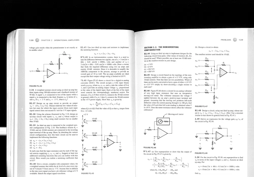
2,43 Figure P2.43 shows a circuit for a digital-to-analog
converter (DAC). The circuit accepts a 4-bit input binary
word ayaa yd, Where dg, 4, 3, and ay take the values of O or
1, and it provides an analog output voltage
to the value of the digital input, Each of the bits of the input
ly numbered switch. For
vo proportional
word controls the corresponding
instance, if a; is 0 then switch $, connects the 20-kQ resistor
und, while if a; is 1 then $; connects the 20-kO resistor
‘ois given by
to
to the +5-V power supply. Show th:
3]
16
where Ris in kQ. Find the value of Ry so that vg ranges from
010-12 volts.
45
20 ka R
eo we
80 ka.
ow
i*
FIGURE P2.43
SECTION 2.3: THE NONINVERTING
CONFIGURATION
2.44 Usin: al op amp to implement designs for the
following closed-loop gains, what values of resistors (Rj, R.)
should be used? Where possible, use at least one 10-K2 resis:
toras the smallest resistor in your de
(a) +1V/V
(o) 42. V/V
(©) +101 V/V
(@) +100 VV
02.45 De
inverting amplifier to obtain a gain of +1.5 V/V, usit
10-kQ resistors. Note that there are two possibilities. Which of
these can be easily converted to have a gain of either +1.0 VV
or 42.0 V/V simply by short-circuit
sign a circuit ba:
ed on the topology of the non-
only
re P2.46 shows a circuit for an analog voltmeter
of very high input resistance tha
moving-coil meter. The voltmeter measures the voltage V
applied between the op amp's positive-input terminal and
ground. Assuming that the moving coi produces full-scale
deflection when the current passing through itis 100 uA. find
the value of R such that full-scale reading is obtained when V
is +10 V. Does the
uses an inexpensive
ter resistance shown affect the voltmeter
(Monel nt
[O--]
FIGURE P2.46
D*2.47 (a) Use superposition to show that the output of
the circuit in Fig. P2.47 is given by
R, R,
X% mit RAIN ms
114 Rk R Rp)
R,
where Ry = Ryl/Ryall - «IR yy and
Ry = RylR, MR lRp
PROBLEMS
(b) Design a circuit to obtain
The smallest resistor used should be 10 kQ.
Rus
ty) o— WW
h k,
ty2 0—AW i w
Rav /
(oO c
Rr
‘ip, oA
Ro
vp, OA
eo
Roy 3
FIGURE P2.47
2.48 Design a circuit, using one ideal op amp, whose out
ULES Up = v4 +3j.~2(v43+30,.)- Hint: Use a structure
similar to that shown in general form in Fig. P2.47,)
2.49 Derive an expression for the voltage gain, vp,
the circuit in Fig. P2.
FIGURE P2.49
2.50 For the circuit in F
vip in terms of the input vol
op amp. For
2.50, use superposition to find
sv, and vs. Assume an ideal
v= 1Osin(2@ x 601) ~0.1sin(2m x 10001), volts
vy = 1Osin(2 x 602) +0.1sin(2x x 10007), volts
G22 CHAPTER 2 OPERATIONAL AMPLIFIERS
20R
AW
e |
4 OW
R z
5 OW
20k
]
-s
FIGURE P2.50
P2,51 utilizes a 10-42
jin amplifier
D2.51. The circuit shown in Fi
potentiometer to realize an adjustable-g
Derive an expression for the gain as a function of the poten-
tiometer setting x. Assume the op amp to be ideal. What is the
range of gains obtained? Show how to add a fixed resistor
so that the gain rang VIN. What should the
resistor value be?
can be 1 (0 21
10-2 pot
FIGURE P2.51
D2.52 Given the availability of resistors of value 1k and
10 kQ only, design a circuit based on the noninverting con-
ration to realize a gain of +10 V/V.
2.53 It is required to connect a 10-V source with a source
resistance of 100 kQ to a 1-k@ load. Find the voltage that
will appear across the load if
(a) The source is connected directly to the load.
(b) A unity-gain op-amp buffer is inserted between the source
and the load.
In each case find the load current and the current supplied by
the source, Where does the load current come from in case (b)?
2.54 Derive an expression for the gain of the voltage fol
lower of Fig, 2.14 assuming the op amp to be ideal exce}
for having a finite gain A. Calculate the value of the closed.
loop gain for A = 1000, 100, and 10. In each case find the
percentage error in gain magnitude from the nominal value
of unity
2.55 Complete the follow
created using one ideal op amp. Note that R,
g table for feedback amplifiers
signifies input
resistance and R, and R, are feedback-network resistors as
labelled in the inverting and noninverting configurations.
case Gin Ry RENEE
a 1ov/V 10kQ |
BO AIWN i)
¢ DVN 100 Ka
o HW
¢ RW rowa
f sw too
t | SVY oa
10 V/V uses an op amp with open-loop gain of 50 V/V and a
Jowest-value resistor of 10 KO. What closed-loop gain actually
results? With what value resistor can which resistor be
shunted to achieve the nominal gain? If in the manufacturing
‘op amp of gain 100 V/V were used, what closed:
process,
loop gain would result in each case (the uncompensated one,
and the compensated one)?
2.57 Using Eq. (2.11), show that if the reduction in the
closed-loop gain G from the nominal value Gy = 1+Rs/R,
is to be Kept less than x% of Go, then the open-loop gain
of the op amp must exceed Gy by at least a factor F
(100/x) = 1 = 100/x. Find the required F for x = 0.01, 0.1,
1, and 10, Utilize these results to find for each value of x the
minimum required open-loop gain to obtain closed-loop
ins of 1, 10, 10°, 10°, and 10° V/V
2.58 For each of the following combinations of op-amp
open-loop gain A and nominal closed-loop gain Gy, calculate
the actual closed-loop gain G that is achieved. Also, calculate
e by which |G| falls short of the nominal gain
the percent
magnitude |G
Case Gy (V/V) AWIV)
a -1 10
b +1 10
c -1 100
d +10 10
e 10 100
f 10 1000
+ 2]
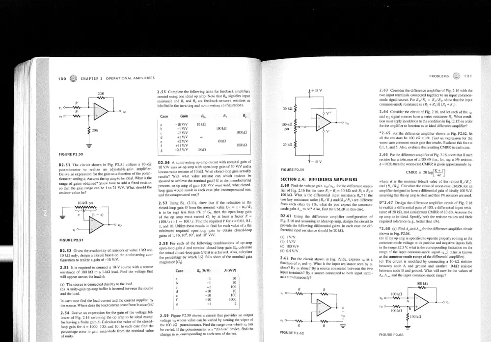
gure P2.59 shows a circuit that provides an output,
5 whose value can be varied by turning the wiper of
the 100-k potentiometer. Find the rar
be varied. If the poten
change in zp corresponding to each turn of the pot
ometer is a “20-turn” device, find the
rou |
EN |
1010S t
pot
204
.-
Yoisv
FIGURE P2.59
SECTION 2.
DIFFERENCE AMPLIFIERS
2.60 Find the voltage gain vp/ v4, for the difference ampli-
fier of Fig. 2.16 for the case R\= Ry= 10 kQ and Ry= R,
100 kQ. What is the differential input resistance R? If the
two key resistance ratios (R/R,) and (R,/Rs) are different
from each other by 1%, what do you expect the common:
‘mode gain A... (0 be? Also, find the CMRR in this ca
02.61 Using the difference amplifier configuration of
Fig. 2.16 and assuming an ideal op-amp, design the circuit to
Provide the followin, ns, In each case the dif-
ferential input resistance should be 20 kQ.
(@ Lviv
() 2v/V
© 100V/V
@ OSvIV
2.62 For the circuit shown in Fig. P2.62, express th as a
function of v, and v4. What is the input resistance seen by 1
alone? By v alone? By a source connected between the two
input terminals? By a source connected to both input termi-
nals simultaneously?
R R
2) OW
4 Oy Ww
R R
FIGURE P2.62
Prostems (9 13
2.63 Consider the difference amplifier of Fig. 2.16 with the
two input terminals connected together to an input common-
mode signal source. For R/R, = R,/Ry, show that the input
common-mode resistance is (Ry + R,) (Ry +R.)
2.64 Con:
and y
the circuit of
2.16, and let each of the x,
ignal sources have a series resistance R,. What condi-
tion must apply in addition to the condition in Bq, (2.15) in order
for the amplifier to function as an ideal difference amplifier?
2.65 For the difference amplifier shown in Fig. P2.62, let
all the resistors be 100 kQ + 1%. Find an expression for the
worst-case common-mode gain that results, Evaluate this For:x=
0.1, 1, and 5. Also, evaluate the resulting CMRR in each case
2.66 Forthe difference amplifier of Fig. 2.16, show that if each
resistor has a tolerance of +100 e% (i.e, for, say, a 5% resistor,
€=0.05) then the worst-case CMRR is given approximately by
K+1
BL de
CMRR = 201
where K is the nominal (ideal) value of the ratios(Rs/R,)
and (R,/R3). Calculate the value of worst-case CMRR for an
amplifier designed to have a differential gain of ideally 100 V/V.
atthe op amp is ideal and that 1% resistors are used,
D*2.67 Design the difference amplifier circuit of Fig. 2.16
to realize a differential gain of 100, a differential input resis
tance of 20 kQ, and a minimum CMRR of 80 dB. Assume the
‘op amp to be ideal. Specify both the resistor values and their
required tolerance (e.g., better than 1%).
"2.68 (a) Find A,andA,, forthe difference amplifier circuit
shown in Fig. P2.68.
() IF the op amp is specified to operate properly so long as the
‘common-mode voltage at its positive and n
inthe ra
ve inputs falls
2.5 V, what is the corresponding limitation on the
range of the input common-mode si 22 (This is known
as the common-mode range of the differential amplifier).
() The circuit is modified by connecting a 10-kQ fesistor
between node A and ground and another 10-kQ resistor
between node B and ground. What will now be the values of
A Acgs and the input common-mode range?
100 kA
100 ka
tno .
100 kA
100 ka
FIGURE P2.68
132 CHAPTER 2 OPERATIONAL AMPLIFIERS
2,69 To obtain a high-gain, high-input-resistance diffe
ence amplifier the circuit in Fig. P2.69 employs positive fee
ative feedback provided by the
back, in addition to the ne
resistor R connected from the output to the negative input of
ly, a voltage divider (Rs, R,) connected
across the output feeds a fraction B of the output, that is, a
voltage Bop, back to the positive-input terminal of the op
amp through a resistor R. Assume that Ry and Ry are much
smaller than R so that the current through R is much lower
than the current in the voltage divider, with the result
B=R,|(Rs + Ry). Show that the differential gi
the op amp. Specifi
n is given by
FIGURE P2.69
2.70 Figure P2.70 shows a modified version of the differ
istor Re
cireuit includes a
ence amplifier. The modifie
which can be used to vary the gain, Show that the differential
(Hi
current through the R, resistors to be
The virtual short circuit at the op amp input causes the
Ry.)
Rk Ry
FIGURE P2.70
D*2.71 The circuit shown in Fig. P2.71 is a representation
of a versatile, commercially available IC, the INA1OS, manu:
factured by Burr-Brown and known as a differential amplifier
module, It consists of
n op amp and precision, laser
trimmed, metal-film resistors. The circuit can be configured
for a variety of applications by the appropriate connection of
terminals A, B, C, D, and 0,
25k 25 kA
AoW
c
BoO—W—#—WW 9 D
25k 25 KO
FIGURE P2.71
(a) Show how the circuit can be used to implement a differ
cence amplifier of unity gain
(b) Show how the circuit can be used to implement single-
ended amplifiers with gains:
i) -1VIV
Gi) +1.V/V
Gi) RVIV
(iy) #12. V/V
Avoid
may act as an “antenna,” picki
through capacitive coupling. Rather, find a convenient node to
ninal in a redundant way. When more thi
eaving a terminal open-circuited, for such a terminal
up interference and noise
connect such a ter
one circuit imp!
tive merits of each, taking in
pendence on comp
lementation is possible, comment on the rela-
.ccount such considerations as
rent matching and input resistance.
2.72. Consider the instrumentation amplifier of Fig. 2.20(b)
with a common-mode input voltage of +3 V (de) and a differ:
cential input signal of 80-mV peak sine wave. Let 2R, = 1 kO,
50k, Ry =R.= 10 kQ. Find the volt
the circuit
2.73 (a) Consider the instrumentation amplifier circuit of
Fig. 2.20(a). If the op amps are ideal except that their outputs
saturate at +14 V, in the manner shown in Fig. 1.13, find the
maximum allowed input common-mode signal for the case
Ry = 1 kQ and Ry = 100 kA.
eat (a) for the circuit in Fig. 2.20(b), and
ince between the two circuits,
2.74 (a) Expressing 1 and xp in terms of differential and
common-mode components, find vy, and vp in the circuit
in Fig. 2.20(a) and hence find their differential component
Xion = to: and their common-mode component !(vo, + von)
Now find the differential gain and the common-mode gain of
the first stage of this instrumentation amplifier and hence the
MRR,
(b) Repeat for the circuit in Fig. 2.20(b), and comment on the
difference between the two circuits
**2..75 For an instrumentation amplifier of the type shown in
Fig. 2.20(b), a designer proposes to make Ry = Ry = R,= 100 kQ,
and 2R, = 10 kQ. For ideal components, what